Like a lot of Hackaday readers, I pride myself on being “the fix-it guy” in my family. When something breaks, I get excited, because it’s a chance to show off my skills. It’s especially fun when something major breaks, like the fridge or the washing machine — repairs like that are a race against time, since I’ve got to get it fixed faster than it would take to hire someone to do it. I usually win the race; I can’t remember the last time I paid someone to work on something. Like I said, it’s a point of pride.
And so when my son came home on Thanksgiving break from his first semester away at college, eager to fire up his Xbox for some mindless relaxation from his biochemistry studies, only to be greeted with a black screen and no boot-up, it was go-time for me. I was confident that I’d be able to revive the dead box in time for him to have some fun. The fact that he’s back at school and the machine is still torn apart on my bench testifies to my hubris, but to be fair, I did get close to a fix, and may still yet get it done. But either way, the lessons I’ve learned along the way have been really valuable and worth sharing.
Diagnosis
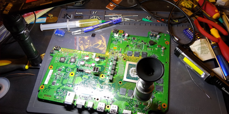
Right off the bat, this looked like a power problem — plug it in, press the button, no LED, no beep, no fan. We checked the basics, like making sure there was line voltage at the end of the power cord and wiggling things around to find loose connections. With those eliminated, I decided that it might be a bad power supply, which on the Xbox One X is an internal module. With teardown instructions at hand, we pulled the power brick out of the case and tested it — 12 V, just like the label says. Too bad — that would have been a simple fix.
A little bit of Googling led me to a series of repair videos that seemed to match the symptoms. One in particular caught my eye; it suggested that a bad HDMI retimer chip could be the culprit. Exactly how this chip would have gone bad was a mystery — the console was largely unused for months — as was how a bad HDMI chip could disable a whole machine. But it was a lead.
Unfortunately, the fix for this problem was far outside my wheelhouse. I’m skilled with a soldering iron, but only in the macroscopic world. Yes, I’ve tried surface-mount device soldering before, going so far as to enter the SMD Challenge at the 2019 Superconference. I didn’t exactly cover myself in glory, but I did well enough with the suboptimal tools on hand at the Supercon that I thought I could probably do a decent job. But first, I’d need to go shopping.
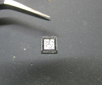
The chip I needed to replace was a TDP158, which comes in a 40-pin quad-flat no-leads (QFN) package. I don’t know much about SMD, but this is clearly a package that can’t be tackled with just a soldering iron. The lands on the underside of the case have a 0.4 mm pitch, and there’s a relatively huge thermal transfer pad that gets soldered to the board. I would need some tools to make the repair possible.
While I was willing to plunk down $55 for a cheap hot-air station on Amazon, I wasn’t ready to shell out for the other tool I’d obviously need: a microscope. I figured — unwisely, as it turns out — that I’d be able to muddle through the repair with the simple head-mounted magnifiers Bil Herd suggested to me back when I explored the issues of getting old as a hacker. The other thing I’d need was a replacement TDP158, which is carried by both Mouser and Digi-Key. Unfortunately, they were both out of stock, with estimated delivery in March — of 2023! Luckily, resellers on Amazon had them in stock, so I added one to my order and completed the teardown while waiting for delivery.
First Repair Attempt
Getting the putatively defective chip off the board was actually easier than I thought it would be. The videos I had watched all had their hot-air stations cranked up to 480°C — that big thermal pad on the back on the QFN really sinks the heat well. It also helps when the chip is being replaced, and you don’t really care how much heat you’re blasting into it. That would come to haunt me later, but for my first go, all I was concerned with was not melting off any nearby caps and resistors, for which I had no spares.
Where I started running into trouble was once the chip was popped free. There’s a big pad underneath which is obviously connected to a lot of copper, because trying to tin it was a nightmare. Just rubbing it with the tip of my Hakko iron wasn’t enough, even with the heat cranked up to the max — the solder would instantly harden and form bumps that would keep the chip well above the surface of the board. And when I used desoldering braid to try to suck away the excess, the braid would just end up soldered to the pad. It took a combination of hot air and soldering iron to get the pads in shape and ready for the new chip.
Everything I had seen on reflow work led me to believe the hard part was behind me; at this point, flux, the solder resist on the board, and the miracle of surface tension would just magically float the chip into the right position with the application of a little heat. And it sort of did, but even through my janky magnifiers, I could see there were problems. The pads along one edge of the chip clearly didn’t have much solder on them, and there were a few obvious solder bridges.
What ensued was literally hours of chasing solder around the board with hot air, my soldering iron with just about every tip I could find to try, several milliliters of flux, and a hell of a lot of swearing. Also a lot of tool changes, especially in the optics department. The head-mounted peepers weren’t enough, so I found a little stand microscope that I could sort of balance above the chip to get a look at the joints. My lighting was also atrocious — I had enlisted my handy Harbor Freight rechargeable work light, which really helped, but it still cast awkward shadows and was in the way of my tools most of the time.
Some Success
I eventually got sick of chasing solder around, and when I was convinced that I had at least taken care of the solder bridges, I plugged enough stuff back together to give the console a test. To my complete astonishment — especially since my son was now watching the proceedings — it booted right up! But alas, when buttoned up and tested on the TV, there was no HDMI output — those solder-starved joints, no doubt. On to round two.
The second time went a little easier thanks to the experience of round one. I popped the chip off, cleaned up both it and the pads, and floated the chip back into position. This time there were no bridges, and all the joints looked bright and shiny — could it be? Did I finally fix it?
Of course not — it wouldn’t even boot this time. I suspect I just plain cooked the chip — between all the solder chasing of the first attempt, and the resoldering of the second try, I dumped a ton of heat into the poor thing and just did it in.
Third Time’s a Charm?
That’s where things stand now, and while I wait for another chip so I can give it a third try, all I can do is look at the lessons I’ve learned. While it’s a poor craftsman who blames his tools, there’s still something to be said for a proper setup. I really need a microscope if I’m going to get serious about this. [Scotty Allen] of [Strange Parts] sings the praises in this video about his microscope, so I might pick up something along those lines. Then again, there are some microsoldering pros who swear by the video-only approach. (Video, naturally.) I think a stereo microscope seems more like my speed, though.
Lighting is another big concern. The scope I’m looking at has a coaxial ring light for shadow-free illumination, but the room lighting in my shop needs an overhaul. Granted, it was built with writing in mind and has mostly task lighting, but being able to dump a lot of light when I need it would be a good idea.
Finally, what I need most is practice. I’ll probably pick up some SMD practice kits, and perhaps some old e-waste to practice desoldering on.
Did I miss anything? Tell us about it in the comments. I’m especially keen to hear about everyone’s experiences climbing the learning curve, especially from old-timers.


Nice article. Repair skills regarding newer chip tech is very important to our community. Like many others I do not like to point out my fails. However learning from ones or others mistakes or misfortunes may be the best learning you can do. I too have attempted repairs of electronics I have no right believing I am skilled enough to tackle. Leaded components I have had a lot of luck with. Lead-less ic’s like BGA, QFN and the like I find exceedingly difficult. Would love to find out how this comes out.
You can accely get away with just heating those chips up and pressing straight down so the solder squishes out, then run a small iron around the “pins” solder paste works better but you can do it with flux. Then you just use some fine solder wic away the extra.
Then after clearing all the extra solder flood it with flux and let it jump into place.
Oh defiantly use leaded solder because of lower melt temp.
YUUUUSSSSSSSSS!!!!!
Lead free standards and regulations are for the companies making millions of devices with billions of solder joints to be thrown away at the first sign of trouble (or in 6 months, depending on device) ending up in the land fill. And that is a good thing that I support….uh the lead free bit, not the cheaply made goods that are over promised and under engineered.
However, supposing proper fume extraction (which isnt hard with a PC fan and some dryer vent tube. Simply smelling some residual is not going to hurt you, dont be a paranoid hypochondriac, the 3 minutes you stand on a street corner waiting for the cross walk or the fumes coming off that 14hr print job, or just being in a car on the freeway exposed you to FAR more ‘harmful particulates’), good ole tin lead flux core solder with a nice eutectic transition, soft and juicy is of ABSOLUTELY NO HARM to the environment. And is a far superior experience, especially for novices. It can easily be argued that regardless of the solder being used the mere act of effecting a repair saves the device as a whole from the dump. Which is logarithmic magnitudes better for the environment than any harm a few lead alloy joints could possibly do. So, dont buy into the lead scaremongering, kiddies. Just because something can be bad for you doesn’t mean you should fear it. Just do some reading, use your mind, do some reasoning (you dont need rubber gloves or a bunny suit, just wash ya hands, ie dont get any in your mouth), and learn to handle potentially harmful materials, safely. Like an adult. Its not hard.
Here’s a good video to reference for this procedure: https://www.youtube.com/watch?v=EaTw_2qQUg8
The main takeaway is to wick away the lead-free solder and put some leaded solder on the pads (and lots of flux) before reflowing. This reduces the heat load that the board and new chip will need for the reflow.
This. And on QFN’s, pre tin the component pads with solder aswell. If you put a little bit to much solder on the thermal pad it isn’t a big issue. Give the chip a gentle push with sharp tool when the solder is melted and the excess will pop out on the side. I have never had a solder bridge between the pads and thermal pad on a QFN.
As a fellow old who fixes everything, I feel your pain. There’s no dancing around it: a good microscope is now as important as a good multimeter. A second hand quality stereo zoom scope like a Nikon SMZ are usually less than 300 US.
As far as viewing equipment, there are lots of options. The usual outlets sell various microscope cameras, either with their own screen or with HDMI output, for a wide array for prices. You can also take a Raspberry Pi DIY webcam with the HQ camera and add a microscope lens to it and attach it to a lamp stand and a monitor. A ring-light or at least a couple of light sources (to remove shadows) will top it off.
I’ve repaired a lot of electronics over the years. And your issue started and ended with assuming you could address that enormous heat sink with heat from the top side only. Modern SMT rework stations address this issue by applying top and bottom side heat at the same time and you will need to do your version of the same.
The easiest at home solution is to use a helper and a second hot air pencil. Have that person direct heat at the bottom while you heat the top.
Thank you, a very timely article for me as I am at a similar stage with my SMT experience and eyesight limitations mean I too am looking at microscopes. There are previous HAD articles but I will be very interested in the comments!
Usually, with thermally capacitative pads on modern large boards, preheating is very, very helpful. Heating the entire board to, say, 100C (i.e. on an IR table) helps, because then you don’t lose as much heat into the board when you heat a section of it. It does have to be even heating, though, AFAIU. Not sure if you’d be able to get a reflow setup like that.
for a microscope get a long working distance model. Having that extra room under it to work is invaluable. I’d also suggest a heater for the bottom side, the idea being to get the whole board up to a temp before solder starts melting so not so much additional heat needs to go into the top side to get things to flow and there is less thermal stress.
Good try and best of luck on the next attempt!
For the last several generations soldering irons have shrunk to accommodate our ever-miniaturized tech. Sometimes it can be nice though to have a big ugly iron for those heavy jobs like soldering ground wires to chasis tabs or as in this case a big pcb heat-sink trace.
I know, you probably don’t want to buy yet another expensive piece of equipment. But I think I only paid about a buck for mine at a local hamfest. I suspect you could find something similar on Fleabay. What you want to look for is big, old and ugly. It will probably have a wooden handle and a power cord that looks like you will get lung cancer if you let it too close to your nose. I don’t have a picture here of mine but it’s similar to one of these: https://www.collectorsweekly.com/stories/233403-vintage-electric-soldering-iron
I’m not entirely sure you can get that onto the pad without harming adjacent pads but if you can it would do the job.
Good Luck!
I keep one around as well, got a reasonably vintage Weller (with a big chunky 45 degrees tilted chisel tip 120W) from my grandfather. He used it to solder zinc gutters. I mainly use it to heat big copper fills to reflowing temps.
I get by dual wielding another solder iron (35W) + regular temperature controlled iron (60W).
These day hot air reflow + temperature controlled iron.
My grandfather left me with a soldering gun but that was a long time ago. He managed to melt iron wire after a long try thinking that it was solder.
Dan,
Type 5 solder paste with a fine dispensing needle and syringe and BUY A METCAL! They have tips fine enough to do the work and can dump enough heat into the joints to solder your PL-259’s without thought. Scour Ebay and the other sites, brand new the price is scary.
Then get the microscope.
When a regularly used device dies suddenly after being unused for time and there’s no obvious indications to go off of, my first instinct is to check the electrolytic capacitors.
Take it into work and do it in your lunchbreak on all the nice tools and proper microscope.
…and experience the stress of the clock ticking away the lunchtime minutes, while in the mean time the prying eyes of colleagues staring at your project and are desperate in giving unwanted tips. Or even worse, ask silly questions. Requiring to explain everything from the beginning… and then the next colleague comes in asking the exact same thing, which the first colleague tries to helpfully answer but leaves out important parts of the story which then lead to confusion which needs to be corrected… then darn, 20 minutes have past.
Then with only ten minutes left on the clock, another colleague comes in, this one has no technical experience and starts to give advice about doing these things at home. So you need to explain that the tools at work are much better for this specific job and that the task itself doesn’t cost the company any money. Then they start talking about their own problems and projects (which although you are not interested in, listen to, because you have to be polite..).
Well better luck tomorrow.
Lunch break repair sessions aren’t always what they could be.
Nailed it!
Looks good! Patience is key! So is a microscope. My first investment was the iron. My second was a microscope with inbuilt light.
Hey, thanks for referencing my video, much appreciated! Sounds like you just need a little bit of practice. To answer a little mystery about why you would have no power with a faulty TDP158 though, it’s because the 5v rail responsible for providing power to the step down converter in charge of generating 3.3v for standby power (for the button press) is also shared with the 5v rail responsible for HDMI power on pin 18, and HPD 5v return on pin 19 of the HDMI port. Certain issues with the chip will put a short on the 5v rail and pull it down to ground, meaning there’s no way for 5v to ever reach the step down converter to generate the 3.3v rail required to turn the console on. Hopefully this makes sense to you, and if you need any pointers I’m at your disposal ;)
Phil (TheCod3r)
The hero we do not deserve. I was wondering why a single chip would render the whole device incapable of powering on.
Can’t see the forest through the trees.
Swapping out chips is fine – if you’re into “shot gun” troubleshooting.
You know, just swap parts and cross your fingers.
The only troubleshooting I read in the article, is checking the 12 volt supply.
What about tracing it through the board ? perhaps to the regulator ?
What about breaking out the o’scope and seeing if you have clock ?
A lot of potential root causes to investigate *before* going through the hassle of swapping out chips.
What you say is true. Another aspect of troubleshooting is researching the case. What problems have other people commonly seen and fixed? For this particular XBox, the HDMI retimer chip is a common failure point, so the author isn’t quite replacing it blindly.
Also, the xbox briefly powering up after the first reflow strongly indicates that the guess was correct.
“it’s a poor craftsman who blames his tools”
I take exception to this. Having been a lot of things in a lot of lives (a woodworker, a mechanic, a stained glass artist, an electronics technician, etc. etc.) I believe that having good high quality tools is a cornerstone of success in every profession.
Not only will a good tool do the job better, but the frustration factor of bad tools will be eliminated completely.
There is the concept of good enough, for the kind of work I do I don’t need a $10,000 scope; but there certainly is the concept of not good enough, and when it comes to reworking SMD there’s a lot of not good enough.
i mean, in sense it is a reasonable saying. but that sense is “you’re a poor craftsman if you show up with inappropriate tools, and then blame them, instead of blaming yourself for being unprepared”.
certainly Dan was attempting this with such a poor setup that I wouldn’t have even attempted it.
To an extent. On paid work that’s true.
Testing one’s tools against a personal job and deciding what needs an upgrade is never a bad idea.
A person that have good skills can compensate (some what) for inferior tools. A person with poor skills won’t go too far even with good tools.
The most important part is to know your limits before you start.
This may not be directly applicable but what I do in soldering down QFN packages with solderable daps is: clean off all the solder, especially on the thermal pad. Turn the chip over and put a tiny dot of solder on its pad. Put a tiny dot of solder on the thermal pad, just enough so it’s definitely not flat. If you have ability to do this, put a heat source under the board. This could be a second hot air pencil with a deflector blowing up on the bottom, or put the board on a hot plate with insulators around the area and a small block of aluminum right on the underside of the chip area that’s sitting on the hot plate to conduct heat through, or something along those lines.
Then use the hot air pencil and watch everything under a scope until you see the thermal pad solder melt. (You can scratch it with the tip of your soldering iron and watch the scratch.) As soon as it melts, place the chip with tweezers and line it up. This way you only dump minimal heat into the chip itself. (The dot of solder on the bottom of the chip will melt and help bond: it’s easy to get a cold/unsoldered joint on the thermal pad and that’ll kill the chip the first time it ramps up to higher power.)
Then get in there with a Metcal STTC145 or other really sharp tip that can go pin-by-pin even on 0.4mm pitch pads and start reflowing each pad until it flows. This is a lot easier with a stereo scope you can tilt at 45 degrees looking into each side of the part.
Thankfully the chips I mostly do have wettable flanks: 0.25mm or so of the pad shows on the side of the part even though it doesn’t stick out, so I can be sure the pins are soldered. If not, and the DAP is ground, you can check continuity pin by pin by measuring the body diode drop between ground and each pin and tell where you need more work before trying to power it up.
It’s possible to do this with solder paste, obviously. I’ve personally had more trouble with the chip pins reflowing and the DAP not reflowing and killing the chip through overheat during use, than I have with setting the chip on a known-melted thermal pad and then going back and reflowing the individual pins.
My brain can’t wrap itself around trying to do QFN soldering for the first time on an Xbox. Which is probably like a 10-12 layer board, lead free solder and buckets of heatsinking capability.
Jeez, you couldn’t’ve picked a worst thing to start off with.
As many others have said – throw down the money on a stereo microscope – as many others of us with again eyes will attest to you will wonder show you got bu so long with out one.
And a stereo microscope can be very useful when removing slivers!
For me, the difference between a stereo microscope and a video one is like night and day. Spend the money and get the stereo, you won’t regret it.
This is why HaD needs like buttons.
>Just rubbing it with the tip of my Hakko iron wasn’t enough, even with the heat cranked up to the max
Once again, “cranking” the set point up does nothing on a temperature controlled iron. If it already fails to reach set point of 300C, turning it to 450C won’t do a thing. The iron’s control system already applies full power at 300C setpoint.
I fought the Battle of SMD as the rest of us, but age and eyesight are where you have to fight it. Binocular optical microscope, electronic microscope…. had good success in the early SMD years, but it gets harder and harder. Gave it up but now look back at old heath-kit products, but hard to find.
Best to lay in plans 10 yrs in advance of the eyes going instead of boldly bulling and building your way through till you hit the brick wall of the eyes.
Pity. Fully equipped lab, huge parts stock, and lotta love for the hobby that was also my career 1976 on.
Have fun now the best you can… it’s gonna get smaller still.
“I suspect I just plain cooked the chip ”
That’s why, when attempting something similar, I usually buy one or two extras, price and availability permitting.
Between my clumsiness and notorious bad luck generally a good idea.
As has been mentioned above, preheating the board is the answer to soldering/desoldering items to heavy ground plane. For preheating, a cheap option is a 1 ring electric hot plate /stove for $20. The type with a ring covered with cast iron, rather than the naked type. In terms of heat they are controllable to well under 100 degrees centigrade or you could, of course, rig up an external thermostat. Can also be used for reflow soldering.
I’ve replaced these retimer chips many many times. If you have the knowledge it’s not so bad, but without it I’d recommend paying a professional.
I have done many HDMI retimer and bga chips if your soldering iron was struggling at tinning the underside of the chip I would recommend throwing the board in a toaster at 160°F and pre heat the board it would help and to remove the lead free solder mix some leaded in with it then use solder wick and board heat good luck. The new cameras with stand alone lens is a neck saver you don’t need a microscope to hook it up to just a monitor
I didn´t read all comments above so maybee someone wrote the same.
Heat up the board first, it stores heat, if it cold you need to heat it up during soldering, (use the air blower, a pan with sand or a kitchen oven), Cover parts arond the HDMI chip with something and you can solder the chip with an hot ai fryer (my prefered method).
Too many time soldering and removing can lead to destroy the chips footprint, some shops offer adapter pcbs, maybee this would be easier, if you solder it on an adapter and the adapter on the board (some are also wired, you can solder under an microscope)
All fixes won´t run forever, but maybee extend the life of the Xbox.
Please tell me more about how you used a hot air fryer to solder in chips!
(Seriously! )
Wow, so glad you found time to help everyone with your valuable tips…. Ugh….
I have had great luck with a $30 usb magnifier that I can hook up to either my phone or pc/pi for tiny soldering such as small vqfn or 201 passives
It is so nice to receive constructive feedback from such a humble person!
The hackaday comments section can be amazingly unpleasant at times.
Well you know what they say. There has got to be at least one douche bag in every crowd. That way the douche is not all over the floor. Thank you Michael for being that bag for us. For without you we may have slipped and fell…
Protect nearby components from the heat gun with tin foil
Teach someone to fish and they will be able to feed themself for a lifetime.
Teach someone they can’t fish and they will feed you until you asset stripped their river and moved on.
You are luck if they proofread their own article. I’ll be able to buy a happy meal if I get $0.10 each time their adlib that are completely wrong.
I literally just did this fix over the holidays. It was the most stressful repair I’ve done to date. I spent a long time in the run up fretting about the process and all the things you have to take off and put on. I probably wouldn’t have tried it had I read your article 1st. I unwisely decided to try the fix with a new Digital microscope with a 7 inch screen . It was better than nothing, but it was very awkward to have to keep looking at the screen. The experience you described about that center pad sucking all heat out of the universe Is spot on. The dang thing wanted to grab my soldering iron. I eventually got the chip back on in a way that looked pretty straight and I borrowed a stereo microscope from work to inspect and fix a couple of bridges. Happily it booted up on first try and it has been working well. The only recommendation I have is that you shouldn’t fret about having perfect arcs of solder from the side of the chip to the pads. If the chip is on straight, there is plenty of contact area below the chip to the pads. The other commenters are right about pushing down on the chip with everything hot to squirt out any excess solder from the center pad.
Good luck with your next go, you got this!
This is far more accomplished than my first effort. Tried installing a modchip to my PlayStation 2 despite never having soldered anything before. Solder went everywhere, took me hours to get it all off, then I dropped the soldering iron whilst holding it above the motherboard and although I caught it in my other hand before it hit, I didn’t catch it by the handle so I received a very large, very painful blister as a prize for my stupidity :)