
No matter what, system architects are always going to have to contend with one – and possibly more – bottlenecks when they design the machines that store and crunch the data that makes the world go around. These days, there is plenty of compute at their disposal, a reasonable amount of main memory to hang off of it, and both Ethernet and InfiniBand are on the cusp of 200 Gb/sec of performance and not too far away from 400 Gb/sec and even higher bandwidths.
Now, it looks like the peripheral bus based on the PCI-Express protocol is becoming the bottleneck, even with advances such as NVM-Express. Or, perhaps more precisely, because of such technologies as NVM-Express for linking flash and soon other non-volatile, persistent storage like 3D XPoint, more directly to the CPU-main memory complex and the attachment of GPU and sometimes FPGA accelerators for compute offload for massively parallel or specialized functions, the PCI-Express bus is getting overloaded.
It is a bit like playing Whack-A-Mole. But the vendors that comprise the PCI-SIG organization that creates and commercializes the PCI-Express bus are not just sitting there are Moore’s Law advances compute, storage, and system interconnect networking at an aggressive pace. The PCI-Express 4.0 protocol hit its Revision 0.0 specification in June of this year, and will be first deployed by IBM in its Power9 processor this year. Neither the new “Skylake” Xeon SP processors from Intel nor the new “Naples” Epyc processors from AMD, both launched within the past month, have support for PCI-Express 4.0, which doubles up the bandwidth over PCI-Express 3.0. But there will no doubt be kickers, probably available next year, that will offer the updated PCI-Express protocol.
Equally importantly, the members of the PCI-SIG are working to double up the performance of the PCI bus again with PCI-Express 5.0, which is slated to have its specification completed by 2019. In fact, back in early June, when the PCI-Express 4.0 protocol spec running at 16 GT/sec was put out in “feature complete” form and was awaiting final approval from vendors to get the Revision 1.0 nod to go to market, the Revision 0.3 specification for PCI-Express 5.0, which runs at 32 GT/sec, was put out at the Revision 0.3 level and is progressing.
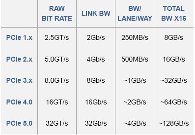
This quadrupling of bandwidth over PCI-Express 3.0, which has a raw bit rate of 8 GT/sec, is necessary so that single-port 400 Gb/sec Ethernet and InfiniBand adapter interfaces can be driven by a single PCI-Express x8 port and not require a jump in networking to x16 ports. GPU and FPGA accelerators need the added bandwidth of PCI-Express 4.0 and 5.0 across the lanes in an x16 port as they will cram an incredible amount of compute and, we presume, larger chunks of HBM memory onto their packages. And, provided that the copper wires are not too short as they support ever-faster signaling, the more capacious PCI-Express available in the future will enable much more tighter coupling of compute nodes using raw PCI-Express switching, and that presents some interesting possibilities and obviates the need in some cases for Ethernet or InfiniBand as a cross-system interconnect on distributed systems.
Just like Ethernet stalled in the jump from 10 Gb/sec to 100 Gb/sec and had to take a ministep at 40 Gb/sec, the peripheral bus hit a region of low air pressure in the jump from PCI-Express 3.0 to PCI-Express 4.0. The flat spot in the exponential curve is pretty obvious in the PCI-Express roadmap:
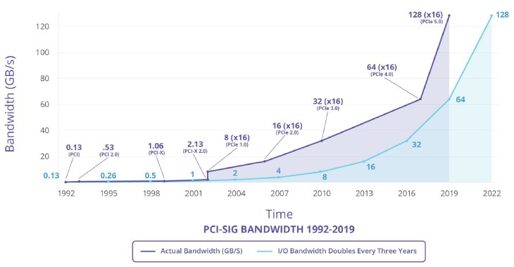
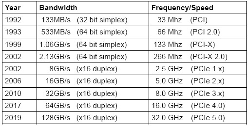
For those of you who like the numbers, here is the evolution from PCI 1.0 through PCI-Express 5.0 in terms of bandwidth and the frequency of the traffic lanes on the bus:
The reason that PCI-Express 4.0 took so long – almost twice as long as usual and longer than any PCI bus jump – is simple: It is really hard to keep driving up capacity on all devices, and no semiconductor process, be it for compute, networking, or storage, can double forever at a lower price per unit of capacity without hitting at least a few snags.
“It gets harder and harder to do each iteration,” Al Yanes, president of the PCI-SIG, explains to The Next Platform. “If you go back to what we said four or five years ago, we have learned a lot, and people have developed different schemes and different ways of doing the PHY. They are using different materials, such as Megtron4 and Megtron6, on the printed circuit board, and are using different connectors. They have also come up with new ways to reduce crosstalk and electrical discontinuities, and with reducing the margining and putting this all together is what makes us fairly confident that we can do PCI-Express 5.0 at 32 GT/sec. People squeeze here and there and innovate.”
The connectors for PCI-Express 5.0 will be a little bit tighter and will have shorter keys and use different materials, but importantly will be backwards compatible with prior PCI-Express 3.0 and 4.0 engineering. That means manufacturers don’t have to change their server motherboard, switch motherboard, or adapter card designs even as they shift to different materials like Megtron4 and Megtron6, which are more expensive but which reduce signal losses, and devices with different tolerances.
The compatibility of PCI-Express 4.0 and 5.0 will be particularly important, since it is fair to say that PCI-Express 4.0 will probably have short life in the field. If IBM rolls out Power9 sometime before the end of 2017, it won’t be shipping it in volume until early 2018. We don’t expect for a lot of PCI-Express 4.0 devices to come to market until Intel’s Xeon SP line supports it. We already know that the “Kaby Lake” Xeon cores do not have PCI-Express 4.0 controllers, but one could be retrofitted into the Kaby Lake variants of the Xeons when they come out around July 2018 or so, bit it might take until the “Cannonlake” Xeons come to market in maybe May 2019 before we see PCI-Express 4.0. A lot depends on how much hay IBM can make with a lead in PCI-Express 4.0 lead.
Generally speaking, there has been a lag of about a year between the PCI spec being finished and PCI products coming to market. The PCI-Express 4.0 spec took a long time to develop, and it is really just now being completed but products have been designed as the spec got closer to completion so IBM won’t be launching Power9 without any peripherals that use the faster protocol. With PCI-Express 5.0, the spec should be done in 2019 and the products should hit the streets in 2020. Yanes says that the move to PCI-Express 5.0 is going to be a bit faster than usual because the PHY is just going to be tweaked and put out the door with minimal changes to the protocol just to get the speed out there.
As for PCI-Express 5.0, which will be using more expensive materials, Yanes says that for a few slots on the server, perhaps to drive networking or GPU and FPGA accelerators, server makers and their customers will be willing to pay a premium for a few of those slots. If we were designing server chips, the lesson here might be to have a PCI-Express 4.0 controller on the chip, but even in 2020 and 2021, maybe it only makes sense to have PCI-Express 5.0 on the package, like Intel is doing with its Omni-Path interconnect on selected Skylake Xeons. We could end up with systems that not only have backwards compatibility, but which literally support two types of controllers at the same time in the system.
Then again, with non-volatile memory and fast networking becoming vital to distributed systems performance, the industry could just try to jump straight to PCI-Express 5.0 in 2020 with tepid support for PCI-Express 4.0. We think this is not likely. The bandwidth demands are too high, to put it bluntly, and in fact, if PCI-Express 4.0 was not delayed so much, it would not have been necessary to create technologies like NVLink in the first place. Nvidia could have just put PCI-Express 4.0 ports and switching and a coherent protocol on the “Pascal” and “Volta” GPUs and have been done with it. The same PHYs that do the 25 Gb/sec “Bluelink” OpenCAPI ports on the Power9 chips are being used to implement NVLink 2.0 and PCI-Express 4.0, after all. In a way, all of the ports on Power9 are PCI-Express 4.0 running different protocol layers on top.
PCI-Express 5.0 uses the same 128/130 bit data encoding scheme that was delivered with PCI-Express 3.0 and 4.0 and, with only 1.5 percent overhead, much better than the 8/10 encoding used with PCI-Express 2.0. With the faster PHYs and the skinny encoding, a 400 Gb/sec Ethernet or InfiniBand port or a dual-port Ethernet or InfiniBand device running at 200 Gb/sec will require 50 GB/sec of bandwidth in both directions on the wire. With PCI-Express 4.0, that would take 16 lanes of traffic (an x16 slot) to deliver around 64 GB/sec, which is sufficient to handle 50 GB/sec of bi-directional traffic. But when PCI-Express 5.0 doubles that up again, this will be accomplished with an x8 slot and that means the form factors will be as they are now for 100 Gb/sec Ethernet and InfiniBand.
If you look at the 400 Gb/sec Ethernet products coming from Innovium and Mellanox Technologies, it would be nice if PCI-Express 5.0 was here next year instead of two years from now. Switching is getting back in synch with compute, but the PCI bus is lagging, and that is not a good thing considering how many things that are moving very fast now hang off of it.


Finally, A Coherent Interconnect Strategy: CXL Absorbs Gen-Z
It is refreshing to find instances in the IT sector where competing groups with their own agendas work together for the common good and the improvement of systems everywhere. So it is with the absorption of the Gen-Z Consortium by the CXL Consortium. With this, CXL has emerged as the …
Counting The Cost Of Under-Utilized GPUs – And Doing Something About It
The compute engines keep changing as the decades pass, but the same old problems keep cropping up in slightly different form. In both the traditional HPC simulation and modeling market and the adjacent AI market including machine learning and data analytics, the GPU has become the compute engine of choice …
For HPC And AI, Composability Might Trump Cheap Flops
Maximizing the aggregate amount of compute that can be brought to bear for any given pile of money is what traditional high performance computing is all about. What happens in a world, though, where the compute environment is not homogeneous and cannot be stuffed full of work by the MPI …
Gen5 x8 for 400GE port? 32G x 8 = 256G, much smaller than 400G and that
doesn’t include inefficiencies. Each direction of 400GE is 400G and each direction
of Gen5 x8 is only 256G.
Well said, and good exposition. Two thoughts:
1. There is probably not enough manufacturing capacity (nor enough product cost budget) to shift all server motherboards to Megtron type materials worldwide. How this evolves will be interesting to watch.
2. Latency is important, not just bandwidth. At some point persistent memory (maybe even shared persistent memory) is going to need to be reached through the CPU’s memory pipeline, not just its (today significantly longer latency) I/O pipeline. There are a lot of ways this could evolve over the next decade, and what the industry does will be determined more by investment choices than by the “technical best answer” (which itself is an elephant viewable from many directions). Again, will be interesting to watch this evolve over the next 10 or 15 years.
Indeed, even 5 years go two trips across the PCI-e bus was a significant fraction of total node to node latency. I suspect this is one of the reasons why Intel is putting Omnipath on chip. I’m hoping that AMD has similar plans or they may find themselves with a significant disadvantage in latency sensitive applications.
Well until PCIe 4.0 and 5.0 at least AMD’s Epyc Platform is offering 128 lanes of PCIe 3.0 for that platform’s 1p and 2P platforms. And:
“FPGA accelerators need the added bandwidth of PCIe-Express 4.0 and 5.0 across the lanes in an x16 port as they will cram an incredible amount of compute and, we presume, larger chunks of HBM ”
There may be entire AMD/Nvidia/Intel/Others’ HPC APUs/SOCs on an interposer using some on interposer types of massively parallel interfaces that do not require clocks higher than 1 or 2 GHz in order to provide very large amounts of effective bandwidth. Take note that AMD has a patent application for some FPGA compute added to the, HBM2/later version, HBM stacks for extra FPGA compute on the HBM stack itself, most likely wired directly with TSVs to the HBM’s memory dies. And the current HBM/HBM2 wired through an interposer etched interface provides 1024 traces per JEDEC HBM stack so an entire computing system made up of modular CPU cores dies and modular GPU dies all wired up via some very wide(Thousands) of traces wide interposer based/etched connection fabric should be sufficient for any CPU to accelerator(FPGA/GPU/DSP/Other processors on Interposer, or MCM) , as well as the HBM memory on MCM/Interposer interfacing. I’d look to maybe computing systems only needing PCIe 4/5 for off interposer/MCM communication and maybe that will be supplanted by optical methods in the future.
There is the current passive Interposer designs that only host passive traces but owing to the fact the the silicon based interposer itself is silicon there will probably be active interposer designs that will host the entire fabric and fabric control circuitry with whatever processor modular units connected by micro-bumps to the active interposer based coherent fabric/system.
Currently systems are still based around mostly separately packaged processor elements(CPUs, GPUs, and other) processors but there will be an evolution towards putting all these separate processors on MCMs or Silicon Interposers, with silicon interposers able to have the maximum amount of parallel traces(And added active circuitry) over any other technology. AMD is so busy currently getting its Epyc line on the market that AMD is not even begun to talk about the next level of professional workstation grade interposer based APU designs that it has in the development pipeline that will probably make use of some on interposer even wider Infinity Fabric derived design that will allow for those much lower/power saving clocks while providing an excess of raw effective bandwidth that we see with JEDEC HBM/HBM2.
I’d look at AMD’s Exascale Interposer white-paper/study(2) discussed to in the NextPlatform article(1) below for some ideas as to what is coming regarding building systems entirely on the interposer from modular CPU chiplets and GPU(Navi, later designs), DSP/other chiplets along with HBM#(Latest) and FPGAs on the HBM Stack/s.
The Exascale systems standards have the strictest power usage regimens and that power savings is very attractive to the cloud/services and server markets also. So at that PCIe 4/5 high clock speeds necessary for more bandwidth over a relatively narrow interface has an intrinsic power usage disadvantage compared to any Interposer etched very wide parallel interface that can replace the high clocks necessary over narrow type interfacing with some wide parallel traces based interfaces that are clocked much much lower.
It’s nice that PCIe 4 is so close to adoption and PCIe 5 should arrive much quicker. But with both Nvidia(Planning for modular GPUs on MCMs and using interposers for some GPUs that use HBM) and AMD(uses both MCMs[Epyc] and Interposers on Vega/HBM), I do not see any long term need for as much PCIe usage for inter-processor communication after the MCM/Interposer based systems begin to be utilized, and HBM will continue to see an increase in usage as currently HBM2 will support 8 GB per stack, with HBM3 expected to provide even more capacity.
The trends being driven by the continued rounds of Government funded exascale research are towards getting all the computing/processing power into close proximity with data. And to make use of more MCM/Interposer multi-processor packaging along with Stacked DRAM/HBM(Next to that processing power) with more massive data-sets held in memory close to where the processing power is there to work on that data, with as little last second data movement/transfer needed until some new data sets are transferred into the HBM2/whatever latest stacked memory to be worked on.
The trends are exemplified by the types of research that is going on to bring compute(CPU, GPU, DSP, FPGA, other processing power) and memory closer together on integrated interposer/MCM packages with HBM2/Stacked memory on the same package and all processing done in a localized fashion over wide parallel memory to CPU, and CPU to other on package processors, connection fabrics, with very little need for any last second staging of any far data until all the computations are completed on the data resident in memory.
This type of processing makes use of the fact the most data transfers will be happening in the background in a non latency critical manner and is done to keep any unnecessary data transfers to and from close memory(HBM/other) from storage(SSD/other) and far memory(DIMM Based) to a minimum and save on power. The only narrow(physically narrow) technology that can match any on package(Interposer, MCM) wide parallel interface power savings over lower(electrically) clocked ultra wide parallel traces types of connection fabrics is Optical, and Optical will be employed to connect up these types of MCM/Interposer based full computing/stacked memory systems. So PCIe for inter-processor communication will not be as needed as it is currently.
I see Nvidia as moving towards the same sorts of APU types of HPC grade SOCs with Nvidia making use of its ARMv8A ISA based/ISA running custom CPU designs and its GPU IP. If Fujitsu can base an Exascale computer on the ARMv8a ISA with SVE extentions, then Nvidia can create an APU llike system similar to what AMD is proposing in the research paper below.
(1)
https://www.nextplatform.com/2017/02/28/amd-researchers-eye-apus-exascale/
and the research paper linked to in the article cane be found here:
(2)
“Design and Analysis of an APU for Exascale Computing
Thiruvengadam Vijayaraghavan†∗, Yasuko Eckert, Gabriel H. Loh, Michael J. Schulte, Mike Ignatowski, Bradford M. Beckmann, William C. Brantley, Joseph L. Greathouse, Wei Huang, Arun Karunanithi, Onur Kayiran, Mitesh Meswani, Indrani Paul, Matthew Poremba, Steven Raasch, Steven K. Reinhardt, Greg Sadowski, Vilas Sridharan
AMD Research, Advanced Micro Devices, Inc.
†Department of Electrical and Computer Engineering, University of Wisconsin-Madison”
http://www.computermachines.org/joe/publications/pdfs/hpca2017_exascale_apu.pdf
“the industry could just try to jump straight to PCI-Express 5.0 in 2020 with tepid support for PCI-Express 4.0”
Is this a fact or just a speculate ? I think the PCIE4.0 will do quite important job to make the PCIE available for the external connection for Rack level solution.
I am kind of confused by your statement of ” he industry could just try to jump straight to PCI-Express 5.0 in 2020 with tepid support for PCI-Express 4.0. We think this is not likely. “.
Do you think the straight jump to PCI-E 5.0 likely or unlikely? Reading through the end of the article I got the feeling that think a direct jump is possible but you made the negative verdict to contradict your further writing.
Actually, for vast majority of users, this is irrelevant :-)))
What consumer electronics need is something like
Ethernet with 300 Mbits/sec (or even 200 Mbits/sec, and no so called full duplex 200Mbis/sec )
USB with 960Mbits/sec (to be called USB 2.4 :-))