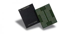
The prototype chip stores 768Gb/96GB of data using the same process technology as is used for 64-layer 3D NAND.
Shipment of prototypes to SSD and SSD controller vendors for evaluation and development purposes started in early June.
The QLC 3D flash memory enables a 1.5-terabyte (TB) device with a 16-die stacked architecture in a single package – the industry’s largest capacity.
Toshiba already mass produces 64-layer 256Gb/32GB devices.
Toshiba has also developed prototype samples of 96-layer 3D NAND using triple-level cell (TLC) technology. Samplesare scheduled for release in the second half of 2017 and mass production is targeted for 2018.
The 96-layer process is expected to deliver 512Gb devices and to use 4-bit-per-cell (quadruple-level cell, QLC) technology, in the near future.
This 96-layer TLC chip will be manufactured at Yokkaichi in Fab 5, the new Fab 2, and Fab 6, which will open in summer 2018.
 Electronics Weekly Electronics Design & Components Tech News
Based on the available information, it is difficult to expect the QLC NAND memory service life to exceed 1000 of the write erase option. More bits in the cell will also require more complex algorithms for write and error correction. Failures of carriers using QLC type memory will be even more frequent than in the case of TLC memory. At the same time, data recovery will become more difficult.