At Hot Chips today, Microsoft's Xbox team unveiled details of the system-on-a-chip (SoC) that powers the newer, slimmer Xbox 360 250GB model. Produced on the IBM/GlobalFoundries 45nm process, it's fair to say that the new SoC (pictured above) is the first mass-market, desktop-class processor to combine a CPU, GPU, memory, and I/O logic onto a single piece of silicon. The goal of the consolidation was, of course, to lower the cost of making the console by reducing the number of different chips needed for the system, shrinking the motherboard, and reducing the number of expensive fans and heatsinks.
The SoC also makes the new Xbox design more power efficient, which is nice for consumers, but the real motivation behind boosting the console's efficiency is to reduce the size and cost of the power supply unit, and to realize the aforementioned savings on cooling apparatus.
Microsoft engineers presented the new SoC and apparently did a lot of the layout (or perhaps all of it) themselves. Given the unique requirement of consoles—the system must perform exactly like the original Xbox 360—and despite a five-year gap and multiple iterations of Moore's Law, the consolidation presented a few interesting challenges.
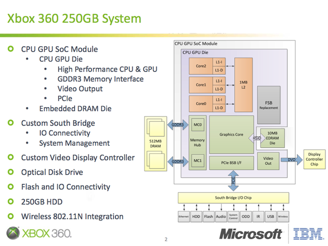
If you take a look at the block diagram above, you'll notice that most of the blocks are fairly obvious: the triple-core CPU is there, as is the ATI-designed GPU, and then you have the dual-channel memory controller and I/O. But the purpose of the "FSB replacement block" may not be obvious. This particular block essentially implements a kind of on-die "frontside bus" with the exact same latency and bandwidth characteristics as the older bus that connected the CPU and GPU when they were discrete parts.
It would have been easier and more natural to just connect the CPU and GPU with a high-bandwidth, low-latency internal connection, but that would have made the new SoC faster in some respects than the older systems, and that's not allowed. So they had to introduce this separate module onto the chip that could actually add latency between the CPU and GPU blocks, and generally behave like an off-die FSB.
Compared to the discrete, 90nm CPU/GPU combo in the original 360 from 2005, the new 45nm SoC draws over 60 percent less power and reduces the total silicon area by over 50 percent. The power and die area savings mean that Microsoft can do with a single fan and heatsink what previously required multiple heatsinks and fans.
The new SoC has only 372 million transistors, which is just not very many by today's standards. For reference, the old 65nm Pentium D 900 from 2006 has almost the exact same number (376 million), while the upcoming 45nm Core i5-760 has almost double the transistor count (774 million). So, despite the fact that the new SoC contains all the silicon brains of an Xbox 360, it's still very svelte by modern standards.
One thing that probably was not a factor in the new design is the infamous "Red Ring of Death" that afflicted earlier iterations of Microsoft's console. That problem has been solved for a while now, so the new SoC approach was really about making the console smaller, cheaper, cooler, and quieter.
reader comments
100