-
IBM's Nicolas Loubet, looking fairly awestruck by a wafer of the new 5nm chips.
-
The ASML EUV machine used to etch the 5nm chips at SUNY. (It's fairly rare to see a EUV machine in the wild.)
-
Wafer washing machines. I don't know why IBM provided this photo.
-
One of the 7nm test chips, created by IBM/SUNY. (Note this isn't a newer 5nm chip; IBM didn't provide a photo of the new 5nm chip.)IBM Research
IBM, working with Samsung and GlobalFoundries, has unveiled the world's first 5nm silicon chip. Beyond the usual power, performance, and density improvement from moving to smaller transistors, the 5nm IBM chip is notable for being one of the first to use horizontal gate-all-around (GAA) transistors, and the first real use of extreme ultraviolet (EUV) lithography.
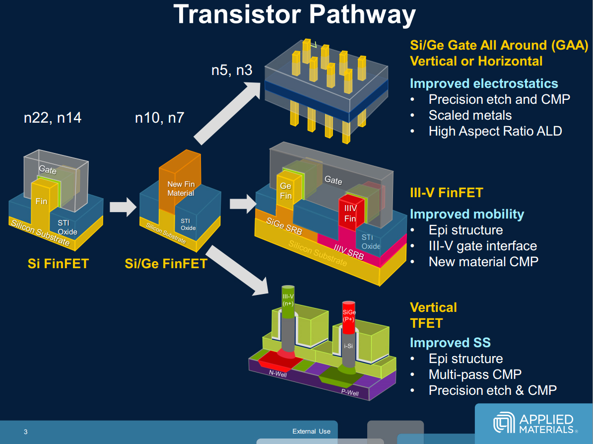
GAAFETs are the next evolution of tri-gate finFETs: finFETs, which are currently used for most 22nm-and-below chip designs, will probably run out of steam at around 7nm; GAAFETs may go all the way down to 3nm, especially when combined with EUV. No one really knows what comes after 3nm.
2D, 3D, and back to 2D
For the longest time, transistors were mostly fabricated by depositing layers of different materials on top of each other. As these planar 2D transistors got shorter and shorter (i.e. more transistors in the same space), it became increasingly hard to make transistors that actually perform well (i.e. fast switching, low leakage, reliable). Eventually, the channel got so small that the handful of remaining silicon atoms just couldn't ferry the electricity across the device quickly enough.
FinFETs solve this problem by moving into the third dimension: instead of the channel being a tiny little 2D patch of silicon, a 3D fin juts out from the substrate, allowing for a much larger volume of silicon. Transistors are still getting smaller, though, and the fins are getting thinner. Now chipmakers need to use another type of transistor that provides yet another stay of execution.Enter GAAFETs, which are kind of 2D, but they build upon the expertise, machines, and techniques that were required for finFETs. There are a few ways of building GAAFETs, but in this case IBM/Samsung/GloFo are talking about horizontal devices. The easiest way to think of these lateral GAAFETs is to take a finFET and turn it through 90 degrees. Thus, instead of the channel being a vertical fin, the channel becomes a horizontal fin—or to put it another way, the fin is now a silicon nanowire (or nanosheet, depending on its width) stretched between the source and drain.
In the case of IBM's GAAFET, there are actually three nanosheets stacked on top of each other running between the source and drain, with the gate (the bit that turns the channel on and off) filling in all the gaps. As a result, there's a relatively large volume of gate and channel material—which is what makes the GAAFET reliable, high-performance, and better suited for scaling down even further.
-
A beautiful series of transmission electron microscopy images showing the stages of building a GAAFET.IBM, Samsung, Global Foundries, et al.
-
This image nicely illustrates the improvement in gate and channel size of a GAAFET vs. a finFET.IBM, Samsung, Global Foundries, et al.
-
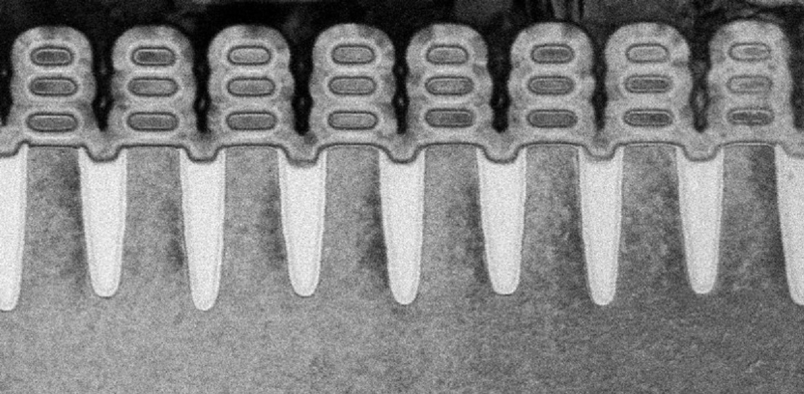
A side-on shot of the completed gate-all-around transistors. Each transistor consists of three nanosheets stacked on top of each other, with the gate material all around them.
One major advantage of IBM's 5nm GAAFETs is a significant reduction in patterning complexity. Ever since we crossed the 28nm node, chips have become increasingly expensive to manufacture, due to the added complexity of fabricating ever-smaller features at ever-increasing densities. Patterning is the multi-stage process where the layout of the chip—defining where the nanosheets and other components will eventually be built—is etched using a lithographic process. As features get smaller and more complex, more patterning stages are required, which drives up the cost and time of producing each wafer.
IBM Research's silicon devices chief, Huiming Bu, says this 5nm chip is the first time that extreme ultraviolet (EUV) lithography has been used for front-end-of-line patterning. EUV has a much narrower wavelength (13.5nm) than current immersion lithography machines (193nm), which in turn can reduce the number of patterning stages. EUV has been waiting in the wings for about 10 years now, always just a few months away from commercial viability. This is the best sign yet that ASML's EUV tech is finally ready for primetime.
So, how good are GAAFETs?
IBM says that, compared to commercial 10nm chips (presumably Samsung's 10nm process), the new 5nm tech offers a 40 percent performance boost at the same power, or a 75 percent drop in power consumption at the same performance. Density is also through the roof, with IBM claiming it can squeeze up to 30 billion transistors onto a 50-square-millimetre chip (roughly the size of a fingernail), up from 20 billion transistors on a similarly-sized 7nm chip.
GAAFETs don't necessarily have the 5nm node sewn up, though. As always with the semiconductor industry, chipmakers prefer to tweak existing fabrication processes and transistor designs, rather than spending billions on deploying new, immature tech. Current silicon-germanium FinFETs will probably get us to 7nm, and the use of exotic III-V semiconductors might take the finFET a step further to 5nm.
At some point, though, it probably won't be worth the time, cost, and complexity of producing ever-smaller transistors and chips. Someone will realise that much larger gains can be had by going properly 3D: stacking dozens of logic dies on top of each other, connected together with through-silicon vias (TSVs). Intel has been looking at chip stacking to mitigate its slow progress towards the 10nm node since at least 2015. Maybe we'll soon see the fruits of that labour; though I doubt they'll be cooled with electronic blood just yet.
reader comments
77