Introduction: PCB Making.


As I was an electronics hobbyist, I always wanted to make a good quality PCB.
Almost all of my projects were done on dot PCB, but some components were such that they couldn't be placed in it because of their pin configurations and size of their leads and many more reasons.
so, the solution for it was to make a printed circuit board. When I started to think about it , I got know that there were 2 types of printing. one is direct transfer of ink from a printout of a laser printer. another is photo resist coating.
when I looked at what I had in my space, I had a inkjet printer.
so instead of spending money on laser printer. I thought I could buy a photo resist coating, which is way cheaper and also I already had access to every materials needed for it. So, in this Instructable I am going to explain how I made a PCB and some tips for good results and good quality .
Step 1: Things You Need.


Photo resist dry film
Photo resist developer
Photo resist stripper
link to buy the above items:
http://www.ebay.com/itm/10pcs-Photoresist-Dry-Film...
ETCHANT
GLOVES
PLASTIC TRAY
LINKS TO BUY THEM:
http://www.ebay.co.uk/itm/PCB-Etching-Starter-Kit-...
http://www.ebay.co.uk/itm/Ferric-Chloride-etching-...
COPPER CLAD BOARD
LINK: http://www.ebay.co.uk/itm/10PCS-70-x-100-Copper-Cl...
UV LEDs
LINK:http://www.ebay.com/itm/100pcs-F5-5mm-Round-Ultra-...
GLASS SLAB
CLIPS TO HOLD SLAB.
OTHER TOOLS:
A Iron Box or A Laminating Machine
A Drill
SOLDERING IRON
A PRINTER
SOFTWARE:
EAGLE or Easy EDA OR ANY OTHER PCB DESIGNING SOFTWARE.
link to download EAGLE:http://www.autodesk.com/eagle-download-win
grab them FAST.
Step 2: Choose Your Photo Resist Type.


There are 3 types of photo resist coating that is paint, spray(POSITIVE) and dry film. you think of and choose yours.
I got a dry film photo resist with a cheaper price.
So I will go with it and explain about how I used it.
A dry film photo resist can be applied to the PCB by either laminating with a Laminating Machine or by ironing.
keep in mind that the temperature must be around 110℃.
take a copper clad PCB board and remove the oxide layer, take photo resist film peel one of the protective layer and place it on the PCB. Gently rub it with your hands and get rid off air bubbles then laminate it with Laminating Machine or Iron box.
Step 3: UV Exposure.


For taking an impression of the layout on the PCB. You should expose the photo resist to UV light under the negative art work of your PCB layout.
you can make your circuits design by using eagle
Take the negative printout on a tracing paper with inkjet out laser printer(both works fine ).
I made a PCB exposure using 45 UV LEDs and attached to a box painted with silver , you can expose it to Sun light in alternative.
it draws 450ma at 12v, I am using 12v 500ma
adopter.
be sure to buy a 390-395 nm UV LEDs or else it wont work.
Suggestions for this step:
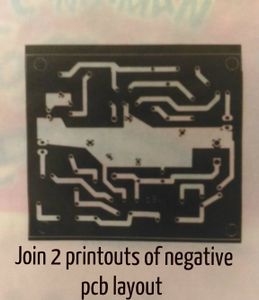
*use 2 printouts one after the other while exposing to UV light.
* expose it to UV light for shorter duration of time like 3~5 minutes if you are using UV LEDs.
Step 4: Developing.


This is the step which shows the past and future.
If this step goes right then you have done all the things right and your next steps Will be done easily.
Use Sodium Carbonate for developing.
mix it with water in ratio 1:100. i.e, for 1gm of sodium carbonate use 100ml of water.
develop until the unwanted areas are got rid off the photo resist.
I failed three times in developing, the reasons are.
*I used one layer of pcb layout while exposing to UV light.
*I didn't laminate the film correctly.
*I exposed the PCB under UV light for longer duration 15~20 minutes.
My suggestion : The developing time depends on the time of UV light exposure. the lesser the time greater the quality of printing.
Step 5: Etching and Stripping.


Use FeCl3 or H2O2 for etching
Use NaOH sodium hydroxide for stripping the photo resist after etching.
make sure your working area is well ventilated while working with etchant and other chemicals. protect your hands with gloves.
Use plastic trays for etching , developing and stripping.
drill holes with suitable drill bits for normal components 0.8mm is enough(like 1/4watt resistor,1/2watt resistor, LEDs , ceramic capacitors and ic's).
solder your components and you have your own homemade quality PCB.
Step 6: Warning........!!!????

Be careful while dealing with chemicals.
Safety first.