At an event today in San Francisco, Intel announced one of the most important pieces of semiconductor news in many years: the company's upcoming 22nm processors will feature a fundamental change to the design of the most basic building block of every computer chip, the transistor.
Intel has been exploring the new transistor for over a decade, and the company first announced a significant breakthrough with the design in 2002. A trickle of announcements followed over the years, as the new transistor progressed from being one possible direction among many to its newly crowned status as the official future of Intel's entire product line.
In this short article, I'll give my best stab at explaining what Intel has announced—the so-called tri-gate transistor. Semiconductor physics are not my strong suit, so corrections/clarifications/comments are welcome. Also, this explanation focuses solely on the "3D" part of today's announcements. Other features of the 22nm process, like high-K dielectrics and such, are ignored. (So if you see a funny term on a slide and you don't know what it means, either ignore it or hit one of the Related Links for more info.)
But before we dive into what's new about Intel's transistor design, we first have to review how traditional transistors work.
Planar transistors and leakage current
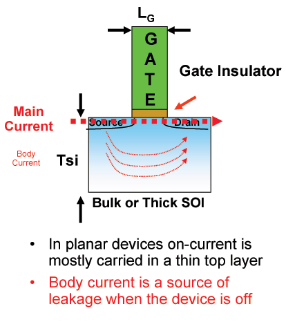
In the diagram above, you can see that a traditional "planar" transistor—the kind that was first invented at the dawn of the microchip era, and which has been the norm up until today's announcement—consists of three main parts: source, drain, and gate. (This is actually one specific kind of transistor, a MOSFET, but let's not get too deep into the weeds.)
The device may look odd, but it's really just an electrical switch. Think of the source and the drain as the two slots in a standard electrical socket; if you stuck a conducting wire (like a coat-hanger ) into both of the slots, you'd close the circuit and current would flow (and sparks would fly, flesh would burn, etc... so don't try that at home.) The transistor's substrate is sort of like a magic wire that can either conduct electricity or not, and the gate is the switch that controls whether the wire will conduct or not.
So when a voltage is applied to the metal plate that forms the transistor's gate, a tiny strip of semiconductor material between the source and the drain (our magic wire) changes from an insulator into a conductor, thereby turning the switch "on" and allowing current to flow from the source to the drain. When the voltage is removed, current stops flowing... or, at least, current is supposed to stop flowing when the switch is off. In reality, trace amounts of current will constantly flow between the source and the drain. This so-called "leakage current" wastes precious power and becomes even more of a problem as transistors get smaller and more numerous.
So to recap, the basic idea is that the transistor is a switch that works because a tiny bit of insulating material between two "electrodes" magically morphs into a conductor when a voltage is applied to it, thereby closing the circuit.
Let's take a look at a different diagram of the same thing:
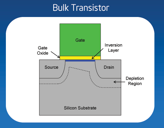
That little strip of blue, the inversion layer, is the region of material near the gate that turns into an electrical conductor when exposed to a voltage. Again, the gate is a small metal plate, and when that plate has a voltage applied to it the layer of semiconductor material that's sandwiched right up against it turns into a conductor.
Now, as transistor gates get smaller, that little strip of blue conducting material naturally gets smaller, and as that little strip of blue gets smaller, less current is able to squeeze through it. When the gate and inversion layer get really small, as they are at the 22nm feature size, that layer can only let a tiny trickle of electrons flow through when the switch is on. But there's already a tiny trickle of (leakage) current flowing through when the switch is off, so the end result is a switch that looks almost the same when it's off as it does when it's on. That's not good, because flipping the switch "on" and "off" is how the chip transmits the 1's and 0's of binary.
There are two main was to fix this problem: 1) reduce the leakage current, and/or 2) force more electrons through that blue conductive strip. Intel's new design does a bit of both, but I'll focus on option 2, because that explains the majority of what's new and important about this advance.
There are two ways to get more electrons through that tiny blue strip. The first and most obvious approach is to crank up the amount of voltage that you apply to the gate, so that the inversion layer will become even more electrically conductive. That's not ideal, though, because more voltage means more power consumption.
The other approach, which is better, is to find a way to make that blue strip even bigger. A bigger blue strip could accommodate more electrical current, and it would do it with less voltage—i.e., you don't need to crank the voltage on the gate up quite so high in order to squeeze more conductivity out of that tiny strip of material, because the strip itself is larger and can transmit more current.
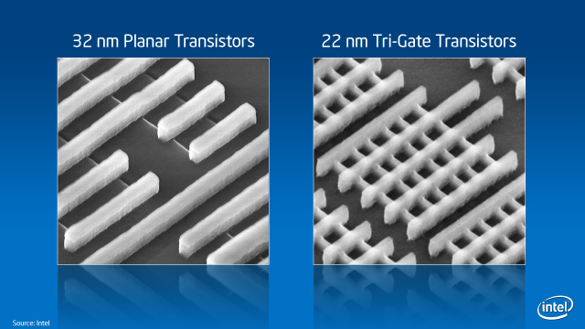
Intel took this second approach, and the chipmaker accomplished this by stretching the gate out into the third dimension.
reader comments
155