 Philips has completed a €23m project to create a production line for vertical cavity surface emitting lasers (VCSELs) for volume photonics applications such as data communications and lighting.
See also: Practical Use For Lasers Found [Mannerisms]
The three year project, called VIDaP, has the backing of the German Federal Ministry of Education and Research (BMBF) and the EU.
Also involved in the VCSEL project are STMicroelectronics and the Technical University of Eindhoven.
VCSELs are specialist compound semiconductor (non-silicon) devices which are traditionally manufactured in small quantities, with largely non-automated processes.
Philips and its project partners now says it has demonstrated how to manufacture VCSELs to the same standards as other high volume semiconductor components.
The company says it has produced 700 million VCSEL’s since the inception of Philips Photonics. It main laser-diode facility is in Ulm, where it aims to further double of capacity by early 2018.
VCSELs are being designed in to industrial and data communications systems, and Philips is predicting potential new applications such as 3D image recognition in smartphones and optical sensors for autonomous vehicle Lidar mapping systems.
Market for lasers
Philips expects the market for these lasers to increase to $1bn by 2022.
Joseph Pankert, general manager, Philips Photonics, writes:
“The market need for VCSELs is rapidly accelerating. Anticipating this demand, over the past few years we have invested consistently in research, product development and efficient manufacturing processes.”
VCSELs are semiconductor laser-diodes, which emit light (1) perpendicular to the surface. The laser consists of active layers, with a thickness of a few nm. In these layers, the electrical carriers are converted into light.
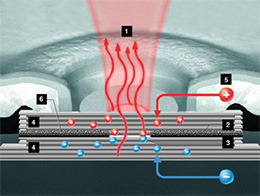
VCSEL structure (Source: Philips Photonics)
Above and below the active layer, multiple layers of alternating refractive index form resonant mirrors (4). The short laser cavity requires a high reflectivity of the mirrors in order to achieve sufficient gain. The doped semiconductor mirrors additionally provide electrical contacts (2) and (3) to the active layers. The size of the active area is defined by the width of an oxidised layer (6) near the active layer.
The layer structure and the vertical light emission make it possible to manufacture lasers in a single growth step. Then standard semiconductor wafer processing steps can be used to define the emission area and provide electrical terminals to the individual laser-diodes.