SnIP shows double helix structure
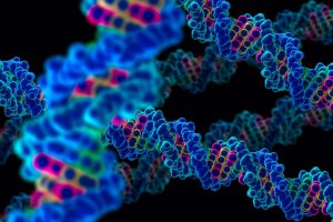
It is a semiconductor with a double helix atomic structure, similar to that which is the basis of DNA. A team from the Technical University of Munich (TUM) has discovered a double helix structure in an inorganic material.
The material comprising tin, iodine and phosphorus is a semiconductor with interesting optical and electronic properties, as well as extreme mechanical flexibility .
It is this structural strength and flexibility which is why why nature codes genetic information similarly in the form of a double helix. Scientists at TU Munich have now discovered an inorganic substance whose elements are arranged in the form of a double helix.
“This property of SnIP is clearly attributable to the double helix,” said Daniela Pfister, who discovered the material at TU Munich. “SnIP can be easily produced on a gram scale and is, unlike gallium arsenide, which has similar electronic characteristics, far less toxic.”
Due to the arrangement of atoms in the form of a double helix, the fibers, which are up to a centimeter in length can be easily split into thinner strands. The thinnest fibers to date comprise only five double helix strands and are only a few nanometres thick. That opens the door also to nanoelectronics applications.
Just as with carbon nanotubes and polymer-based printing inks, SnIP double helices can be suspended in solvents like toluene. In this way, thin layers can be produced easily and cost-effectively. “But we are only at the very beginning of the materials development stage,” said Daniela Pfister. “Every single process step still needs to be worked out.”
Since the double helix strands of SnIP come in left and right-handed variants, materials that comprise only one of the two should display special optical characteristics.
This makes them highly interesting for optoelectronics applications. But, so far there is no technology available for separating the two variants.
 Electronics Weekly Electronics Design & Components Tech News

