It works for indium phosphide, but not for silicon – yet.
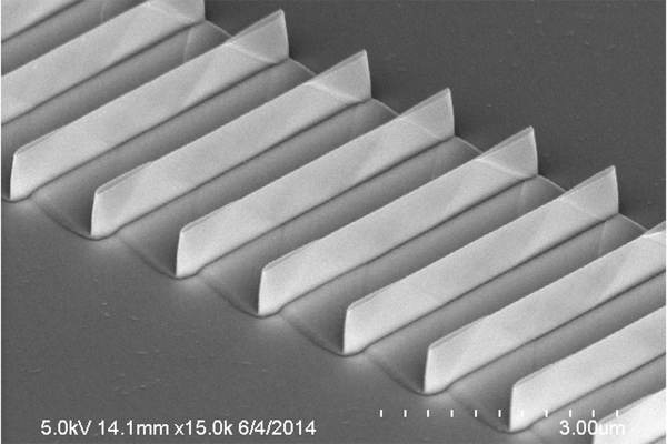
The aim was to etch tall fins with vertical sides and few surface blemishes, and build a suitable transistor on the high aspect-ratio fins.
“We use a technique that gives a much higher aspect ratio, and the sidewalls are nearly 90 degrees, so we can use the whole volume as the conducting channel,” said researcher Yi Song. “One very tall fin channel can achieve the same conduction as several short fin channels, so we save a lot of area by improving the aspect ratio.”
The smoothness of the sides is important, he added, since the fins must be overlaid with insulators and metals, and to have consistent performance the interface between semiconductor and insulator needs to be smooth and even.
Illinois is using is metal-assisted chemical etching (‘MacEtch’), in which a metal template applied to the surface acts as a catalyst for a liquid chemical etch. In particular, it is inverse MacEtch (i-MacEtch) where the metal acts as a catalyst to initiate etching on the exposed semiconductor surfaces, rather than the material covered by the metal.
 “Typically, finfets are made by ion beam etching, which has a number of challenges, said Li: Creating fins with sloping sides is one, where only the top edge can be used for the transistor. Another is surface damage which paves the way to leaky transistors.
i-MacEtch works with a layer of gold on InP, and sadly gold is incompatible with silicon processing. “However, they are working to develop a MacEtch method that does not use gold,” said the university.
The team has published results as ‘Ultra-high aspect ratio InP junctionless finfets by a novel wet etching method‘ in Electron Device Letters.
Junction-less transistor?
According to the published paper, conventional inversion-mode finfets are not ideal technology for very tall thin fins (the team is working at up to 50:1 aspect ratio) because the necessary deep source and drain doping profiles require ion implantation followed by annealing at a level which might not repair lattice damage before the thermal budget is used up – and there are other issues relating to doping uniformity and source-drain punch-through.
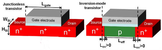 The junction-less transistor, invented at Tyndall National Institute of the University College Cork does not require lateral p-n junctions at the source and drain (see diagram).
Instead, the channel of the junction-less transistor has the same doping as the source and drain (see diagram) so there are no junctions at either end of the channel. The gate is doped opposite to the channel, and it is the effect of this that depletes carriers from the channel – creating an off-state when the gate s not biased. There is an excellent presentation on the concept here.
Crucially, the channel has to be thin enough to be completely depleted, as it can be in a thin tall fin.
Indium phosphide junction-less finfets were created with 63mV/decade sub-threshold slope and 3×10⁵ on-off ratio.
Why tall fins?
Tall fins, providing much of the height can be used as channel, can replace multiple shorter fins and therefore achieve the same on-resistance with a smaller footprint on the die.