
Abstract
The facile generation of hierarchical CdS films and their accompanying application comparison as efficient photocatalytic electrodes toward water splitting were successfully achieved in this study. Three hierarchical CdS films, including nanoparticle packing film (CdSP), neat film (CdSN) and homojunction film (CdSH) deposited on an indium tin oxide (ITO) substrate, were realized by virtue of chemical bath deposition (CBD), atomic layer deposition (ALD) and the well-programmed combinational deposition (PCD) protocol with the above two processes successively. The experimental details demonstrate that the CdSH film acquired from PCD affords an amazing photocatalytic boost toward water splitting, which may profit from the larger surface area and from better absorption. The adoption of CdSH film as a photocatalyst can result in up to 22.18 times or 3.34 times the enhancement of the photocurrent density compared to reference devices with a CdSP or CdSN photoelectrode, indicating the effectiveness of the excogitation of the programmed protocol. Ultraviolet photoelectron spectroscopy was utilized to elucidate the electronic structures of the CdSH bilayer photoanode, and the dependence of their directional photocurrent on the energy level alignment was also depicted. This work not only excogitates the programmed deposition protocol that may be facilely extended to the fabrication of other hierarchical nanomaterials but also gives prominence to the importance of morphology and interfacial energetic control toward enhancing catalytic efficiency.
Export citation and abstract BibTeX RIS
1. Introduction
Securing the availability of sunlight as a renewable energy of sufficient scale to replace fossil fuels is one of the great challenges of the 21st century [1]. The direct conversion of solar energy into storable fuels in a photoelectrochemical (PEC) water-splitting cell has the potential to satisfy this requirement. A PEC cell toward harvesting sunlight, first demonstrated by Honda and Fujishima, is composed of a TiO2 semiconductor photoelectrode and a Pt counter electrode [2]. Thereafter, various TiO2 semiconductors with different nanostructures as photocatalysts have been studied as particularly appealing candidates for practical applications due to their low cost, abundance and stability toward corrosion [3–11]. Impressive as this is, however, compared with the abundant visible light (which contains ∼45% solar energy), the typical photocatalyst of TiO2 still has practical limitations due to the requirement of near ultraviolet (UV) irradiation (just ∼4% in the solar spectrum) for efficient photocatalysis [12, 13]. Therefore, the development of efficient visible-light-absorbing photocatalysts is highly needed to meet further renewable energy resource and environmental requirements.
In terms of the band gap magnitude and the position of the band edges (∼2.4 eV), which correspond well with the solar spectrum, CdS is ideally suited for photocatalytic water splitting [14, 15]. The photocatalytic efficiency of CdS is substantially influenced by various factors such as surface area [16], cocatalysts (e.g. Pt, Ni) [17, 18], support materials (e.g. TiO2, ZnO, MoS2, PbS, Al2O3, graphene oxide, a carbon nanotube or titanate nanosheet) [19–26], etc. Despite its great deal of promise, one remarkable fact needs to be identified, which is that most reports involve a nanostructure carrier to accomplish the water splitting process such as a nanotube [27], nanosheets [28] or microspheres [29]. Rare systematic research has been reported that focuses on the impact of bare CdS nanofilms with a versatile hierarchical structure on the photoelectrochemical performance of water splitting.
Inspired by the aforementioned issues, we have constructed three hierarchical CdS films herein on the basis of the considerations of the morphology and the interfacial energetic element to serve as an efficient PEC photoelectrode toward water splitting. As we know, morphology control has great influence on material properties and thus leads directly to a different photocatalytic efficiency. For instance, geometries generated with a larger surface-to-volume ratio will decrease the distance over which the charge transport has to occur and will increase the amount of available surface area for catalytic reactions [30–33]. Therefore, by virtue of the simplicity and low cost of atomic layer deposition (ALD) and the accuracy control in the thickness and morphology of chemical bath deposition (CBD), the CdS neat (CdSN) film and CdS NP packing (CdSP) film were facilely prepared in this work. In order to preferably acquire nanofilms, a programmed combinational deposition (PCD) protocol on the basis of complementary advantages of ALD and CBD was also achieved toward the fabrication of a CdS NP neat-film homojunction (CdSH) film (figure 1). The nanoparticles constructed in the CdSH film provide a larger surface area for a more efficient catalytic reaction, which also enhances the charge separation and suppresses the charge recombination at the interfacial region. By virtue of this superiority, the employment of CdSH as a photoelectrode for PEC water splitting significantly results in 22.18 times or 3.34 times the photocatalytic current density compared to the CdSN or CdSP film.

Figure 1. Schematic for the preparation of CdS films via (a) the chemical bath deposition (CBD) process, (b) the atomic layer deposition (ALD) process and (c) the programmed combinational deposition (PCD) protocol with the CBD and ALD in proper sequence.
Download figure:
Standard image High-resolution image2. Experimental section
2.1. Fabrications of materials and photoelectrodes
Cleaned glasses with a capped 100 nm ITO layer were pre-cleaned in an ultrasonic cleaner with acetone, ethanol and de-ionized (DI) water in sequence. After being dried with nitrogen, three types of samples were fabricated by the ALD process, the CBD process and the programmed protocol with the above two approaches in proper sequence.
In detail, the neat film (CdSN) deposited by the ALD process was prepared according to our previous work [34]. Typically, the ALD growth process of polycrystalline CdS films on ITO substrates was performed under optimum operating conditions using dimethyl cadmium (DMCd) and in situ generated H2S precursors. The process pressure was 2*10−1 torr with high-purity N2 (flow rate = 10 sccm) as the carrier and purging gas. The optimized ALD cycle settings for CdS films were followed with a 0.015 s pulse of H2S, a 10 s purge of N2, a 0.015 s pulse of DMCd and a 10 s purge of N2. The thickness of the ALD-deposited CdS films per cycle was determined to be 0.35 Å by an Alpha-SETM Spectroscopic Ellipsometer. 3000 ALD cycles were carried out, and the film's thickness was calculated at 105 nm. As demonstrated previously [35], the growth rate of the CdS films is self-limited and will be saturated with respect to the DMCd pulse time of 0.4 s, and the N2 purge time of 10 s is sufficient to remove the excess reactants.
The preparation of CdS nanoparticle packing (CdSP) film by the CBD process was carried out by vertically immersing the ITO glass substrates inside of a Bunsen beaker. The precursor solutions used in this work were prepared by mixing 0.025 mol L−1 Cd(NO3)2, 0.15 mol L−1 sodium citrate, 0.05 mol L−1 thiourea and DI water, with concentrated ammonia with a volume ratio of 2% to adjust the pH value. In the CBD process, the bath was covered for stabilizing the temperature and reducing the loss of ammonia. After deposition, the substrates were dried by flowing N2 and annealed on a hot plate at a certain temperature in air. The film thickness of the CBD-grown CdS was controlled at 300 nm. During the CBD process, the bare sides of the ITO glass substrates were covered with tape to prohibit the growth of CdS films.
The third sample was a dual band gap homojunction (CdSH) thin film deposited by the proper programmed combinational deposition (PCD) protocol with CBD and ALD processes, successively, and was named CdSH. The thicknesses of the CdS constructed in the CdSH film prepared by CBD and ALD were controlled at 300 nm and 105 nm, respectively, the same as that of the pure CdSP and CdSN films. Therefore, the total thickness of the CdSH film is 405 nm. After the CdS films were deposited on the clean ITO substrate by the three approaches, respectively, acrylic modified epoxy glue was used to cover the surface of the CdS layer to control the size of the area exposed in the solution.
2.2. Characterization and measurements
The thickness of the CdS nanofilm was calibrated by the Alpha-SETM Spectroscopic Ellipsometer. The surface morphology was characterized with a scanning electron microscope (SEM). The UV–vis absorption of the sample was recorded at room temperature with a PerkinElmer LAMBDA 750 UV/Vis/NIR spectrophotometer. The crystal structure was analyzed by a PANalytical Empyrean multifunctional x-ray diffractometer (XRD) with the incident angle (ω) at 0.6. The elemental composition and the electronic structures of the films were determined by ultraviolet and x-ray photoelectron spectroscopies (UPS and XPS) in a Kratos AXIS Ultra DLD ultrahigh vacuum system (with a base pressure of 3 × 10⁻¹⁰ torr) with HeI excitation (21.22 eV for UPS) and a monochromatic Al Kα source (1486.6 eV for XPS).
2.3. PEC measurements
The photoelectrochemical (PEC) cell properties were examined by a typical three-electrode system (660D Electrochemical Workstation (CH Instruments)) with a silver-silver chloride reference electrode and a Pt counter electrode. The CdS thin film grown on the ITO substrate was tested as a working electrode in a 1 M Na2S aqueous solution. The exposed area was controlled by means of acrylic AB adhesive coating on the surface of the sample. Also, the simulated solar illumination was contributed by a xenon lamp (spectra region: 300−800 nm), which provided uniform illumination and self-adjusting intensity.
3. Results and discussion
The deposition process of versatile hierarchical CdS nanofilms on an ITO substrate is schematically depicted in figure 1, which vividly represents the formation of CdS films with a different model. For instance, only several CdS crystal nucleuses on the surface of the substrate were deposited at the primary stage of the CBD process. More crystal nucleuses shaped and grew up until a complete CdSP film was formed, as shown in figure 1(a). In contrast, the CdSN film was shaped in all of the ALD stages (figure 1(b)). By virtue of the PCD protocol with the CBD and ALD processes in proper sequence, the CdSH films were further facilely generated.
Figures 2(a)–(c) shows the top-view SEM images of the resulting CdS films. The particle sizes in the CdSP film were clearly found to vary widely from 110 nm to 320 nm (figure 2(a)), whereas the CdSN film with a small roughness of about 2 nm was demonstrated, which corresponds to our previous work [34]. In the CdSH NP-film, an approximately 300 nm thick CdSp film was well wrapped by the CdSN film through regulating the experiment process. From figure 2(c), we can see that the morphologies of CdSH are semblable to the CdSP film due to its 3D conformation, indicating that the ALD layer can coat the uneven surface completely and uniformly. The roughness of the films can be seen from the cross-section SEM images inset in figures 2(a) and (c). In addition, the hierarchical structure of the CdSH film can obviously be seen from the cross-section SEM image under higher magnification (figure S1).
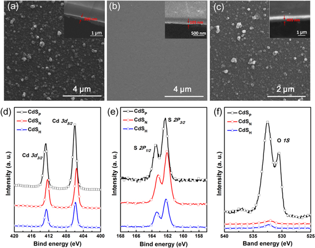
Figure 2. (a)–(c) SEM images of CdS films on an ITO substrate with different deposition methods of CBD, ALD and PCD, respectively. The insets are the corresponding cross-section SEM images of different CdS films on an ITO substrate. (d–f) XPS core level spectra with Cd 3d, S 2p and O 1s of the CdSP, CdSN and CdSH films, respectively.
Download figure:
Standard image High-resolution imagePreviously, we have demonstrated that the Cd 3d and S 2p core level spectra can verify the success of the ALD process, and the quantitative analysis of the element composition is easily calculated by the x-ray photoelectron spectroscopy (XPS) measurement [34]. Herein, the XPS results for the Cd 3d and S 2p core levels in the resulted CdS films were also provided in figures 2(d)–(f). According to the quantitative analysis of the Cd 3d and S 2p core level spectra, the atomic ratio Cd-to-S of CdSN was determined to be approximately 1.62:1, and the ratio of CdSP was about 2.07:1. Regarding CdSN, for instance, the Cd 3d spectrum exhibits double peaks at 412.4 eV and 405.6 eV due to the 3d 3/2 and 3d 5/2 peaks with a separation of 6.8 eV, which is typical in CdS-based materials. Meanwhile, the S 2p 1/2 and 2p 3/2 peaks appear at 163.4 eV and 162.2 eV, supporting the conclusion that the chemical composition of the Cd and S elements results in CdSN film formation. By comparison, from figures 2(d)–(f), we can see that the core level spectra of CdSH are the same as CdSN without the existence of plentiful oxygen. These results, as well as the semblable morphology of CdSH and CdSP, prove that CdSP was well wrapped by the CdSN.
The x-ray diffraction (XRD) characterization of different CdS films deposited on the ITO substrates was also conducted, as shown in figure 3(a). Due to the sulfur vacancies, the on-stoichiometric structure of the CdS films exhibit a polycrystalline structure, which is different from the typical zinc blende (cubic) and wurtzite (hexagonal) crystals of stoichiometric CdS. As reported in the literature, the polycrystalline CdS film prepared by the ALD method is a mixture of zinc blende (cubic) and wurtzite (hexagonal) crystals, and the transition between these two phases strongly depends upon factors such as the deposition method, the temperature, the time and precursors [36]. In this work, it's hard to find any slight difference between the spectra of the CdSN film and ITO substrate from figure 3(a). The possible reason is that the CdSN film is too thin to be detected. By comparison, it is evident that the CdSP films are endowed with obvious spectra changes. The spectral lines clearly rise from 25° to 30° compared with the reference of the ITO substrate. In order to eliminate the interference of the ITO substrate, the same method was also used to deposit CdS thin film on the glass directly, as shown in figure 3(b). The changes during the angle from 25° to 30° are still easy to find. The other two regions of variation can also be caught without the ITO patterns' interference. For the purpose of extracting the lattice plane information, we increase the thickness of the CdSP film to get well-shaped features. As shown in figure S2, the peaks at 2θ = 24.9°, 26.8°and 28.3° are assigned to the (100), (002) and (101) planes of the hexagonal CdS structure, respectively. The other two areas with 2θ values at 43.9° and 51.9° are assigned to the (110) and (112) planes. In addition, the peaks at 26.8° and 43.9° can be assigned to the (002) and (110) planes of the hexagonal structure or the (111) and (220) planes of the cubic CdS structure. Therefore, we can conclude that the polycrystalline CdSP film is the mixture of zinc blende (cubic) and wurtzite (hexagonal) crystals. In addition, the spectra of the CdSH film and the CdSP film after the elimination of the ITO influence (figure 3(a)) are similar to that on the glass substrate (figure 3(b)), indicating the similar polycrystalline structure.
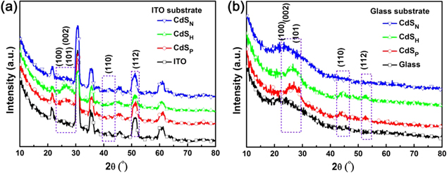
Figure 3. X-ray diffraction patterns of different CdS films on (a) ITO substrates and (b) glass substrates.
Download figure:
Standard image High-resolution imageGiven the importance of PEC cells as solar energy conversion devices, the applications of the acquired CdS thin films as photoanodes in the PEC water splitting process were conducted. The corresponding current density-voltage (I-V) characteristics are compared in figure 4. The potentials are reported versus both the Ag/AgCl and reversible hydrogen electrode (RHE), in which the RHE are obtained using the formula  . By precise measurement, the pH value of a 1 M Na2S aqueous solution is about 13.6. Therefore, the different potential between the Ag/AgCl and RHE is 1 V. From figure 4(a), the CdSP film was observed to perform better than the CdSN film under the same intensity illumination. When the potential versus Ag/AgCl is at zero, we can see that the current densities of the CdSN and CdSP photoelectrodes are 0.096 and 0.632 mA cm−2, respectively. Also, the current density of CdSH is 2.143 mA cm−2, which is about 22.18 times or 3.34 times greater than that of CdSN or CdSP, respectively. The I-V characteristics of the CdS film with three morphologies were also conducted under different power illuminations of 100, 292 and 385 mW cm−2, as shown in figure 4(b). The experimental details show that even under different power illuminations, the CdSH photoelectrode displays the best performance compared to CdSN or CdSP, indicating the significant advantages of CdSH films.
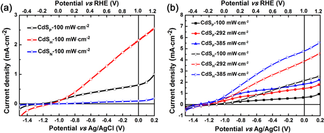
Figure 4. Photocurrent versus the voltage of CdS films in 1 M Na2S (a) with different deposition processes and (b) under various illuminations.
Download figure:
Standard image High-resolution imageTo justify enhancing the photocurrent density, a series of I-V characterizations for the CdS films with different thicknesses were also conducted. Figure 5 shows the I-V results of versatile CdS film electrodes with thicknesses of 105 nm, 300 nm and 405 nm, respectively. From figure 5(a), we can see that with the increase of the thickness of the CdSN film from 300 nm to 405 nm, the short-circuit photocurrent density (Isc) decreases gradually from 0.099 mA · cm−2 to 0.014 mA · cm−2. In contrast, the Isc of the CdSP photoelectrode displays a growth tendency from 0.39 mA · cm−2 to 0.82 mA · cm−2 upon the increase of the film's thickness (figure 5(b)). Nevertheless, from table 1 and figure S3, the Isc with the CdSP film as a photoelectrode (0.82 mA · cm−2) can be seen far less than that of the CdSH photoelectrode (2.15 mA · cm−2) with the same thickness of 405 nm. Therefore, a sufficient justification can be drawn that the enhancement of the photocurrent density benefits from the well-programmed combinational deposition (PCD) protocol rather than the increase of the film's thickness.

Figure 5. Photocurrents versus voltage in a 1 M Na2S solution of (a) CdSN and (b) CdSP photoelectrodes with different thicknesses.
Download figure:
Standard image High-resolution imageTable 1. The short-circuit photocurrent density (Isc) of versatile CdS film electrodes with different thicknesses.
| Isc (mA · cm−2) | |||
|---|---|---|---|
| Samples | 105 nm | 300 nm | 405 nm |
| CdSN | 0.099 | 0.021 | 0.014 |
| CdSP | 0.39 | 0.64 | 0.82 |
| CdSH | — | — | 2.15 |
As reported, the process of photocatalytic water splitting contains three main steps: (1) the absorption of photons to form excitons, (2) the charge separation and migration to the surface reaction sites and (3) the construction of surface reaction sites for hydrogen/oxygen evolution [36]. We proposed that there are two crucial factors that affect the efficiency of the photocatalyst: surface area and the absorption of the CdS films. The photoelectrode of the CdSH film, which consists of innumerable small CdS grains, have larger surface-area-to-volume ratios and reduce the distance for the photogenerated holes that migrate to active sites on the surface. The electron transport rate in CdSH NP-films is much lower than that in a bulk single crystal due to the large number of trap states at the grain boundaries, resulting in an insignificant charge recombination in the CdSH film photoelectrodes [8]. In addition, the suitable forbidden bandwidth and thin film's thickness guarantee a response with the simulated visible light of the solar spectrum, and more excitons will be excited. Figure S4 indicates that the CdSH have the best absorption, and the CdSP exhibit far better absorption properties than CdSN, which is in accordance with the difference of their efficiency.
Further investigations for the rest of the field, to increase the photocatalytic efficiency, suppress the recombination at boundaries and defects, and separate more charge carriers for charge migration to surface reaction sites were conducted.Further experiment was designed and applied herein to research the charge carrier collection efficiency of three CdS films in the water splitting process. The photocurrent densities for all three types of film photoelectrodes under various illuminations were characterized to study their response to intensity light. When increasing the illumination intensity, the small cathodic shifts of the onset potential of CdSN for PEC water oxidation can be observed from figure 6(a), whereas the changes of the onset potential cannot be recognized with ease in either the CdSP or CdSH films (figures 6(b) and (c)). This may be ascribed to the higher conduction band edge of CdSN compared to CdSP. From table 2, we can see that higher-intensity light leads to a stronger response, and the current density of the CdSH photoanode rises from 2.148 (under 100 mW cm−2 illumination) to 4.790 mA cm−2 (under 385 mW cm−2 illumination) with a voltage of ∼1 V versus RHE. By comparison, although the CdSN film does not present excellent efficiency, it can bring a remarkable enhancement in the current density. When integrated with the CdSP film, the value of the enhancement is larger than that of pure CdSN neat film. It may ascribe to two contributions of the CdSN film: the increase of optical absorption after the deposition of CdSN (figure S4); or the location changes, which is of benefit for charge carrier separation. From figure S4, we can draw a conclusion that the band gap of the CdSN film (2.4 eV) is narrower than that of the CdSP film (2.5 eV). Moreover, the cutoff edge of the CdSH has an obvious red shift after the ALD process, resulting in a broader response region to the simulated solar spectra.
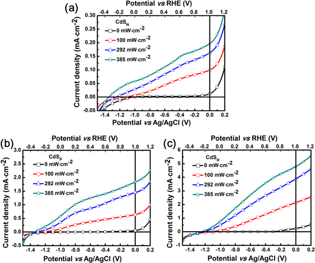
Figure 6. Photocurrent versus voltage in 1 M Na2S under various intensity illuminations of (a) CdSN (b) CdSP and (c) CdSH films.
Download figure:
Standard image High-resolution imageTable 2. The current densities of three types of CdS nanostructures as photoelectrodes under different illuminations with a voltage of ∼1 V versus RHE (∼0 V versus Ag/AgCl).
| Isc (mA cm−2) | |||
|---|---|---|---|
| Sample | 100mA cm−2 | 292mA cm−2 | 385mA cm−2 |
| CdSN | 0.099 | 0.163 | 0.197 |
| CdSP | 0.635 | 1.444 | 1.835 |
| CdSH | 2.148 | 3.889 | 4.790 |
To quantitatively address the photoactivity of CdS electrodes, IPCE measurements were performed to study their photoresponse as a function of the incident light wavelength (figure 7(a)). IPCE is expressed as IPCE = (1240I)/(λJlight), where I is the photocurrent density, λ is the incident light wavelength and the Jlight is the incident light power density. The IPCE of the CdSH electrode is around ∼19% across the absorption ranges, which are higher than that of the CdSP (∼7%) or CdSN (∼1.2%) electrodes, indicating that the electron-hole pairs are separated more efficiently in the CdSH electrodes. All of the samples have a pronounced IPCE at the wavelength up to 500 nm; then, the IPCE dropped to a minimal level at a wavelength below the CdS band gap energy of ∼550 nm (band gap of the bulk CdS, 2.3 eV). In addition, the lower IPCEs registered in the UV region instead of the visible region may attribute to the insufficient UV penetration, as UV light is more scattered and absorbed than visible light, and UV light is substantially absorbed by the ITO substrate [37].

Figure 7. (a) Incident photon-to-current conversion efficiency (IPCE) spectra of the CdS photoelectrode at a potential of 0 V versus Ag/AgCl. (b) Time-dependent photocurrent test measured with the potential bias of 0 V versus Ag/AgCl and 100 mW · cm−2 continuous light illuminations.
Download figure:
Standard image High-resolution imageIn addition, the photocurrent versus time (I-t) curves were recorded under continuous light illumination to indicate the stability of the electrodes. As shown in figure 7(b), after illumination for 600 s, the photocurrent density decreased by 36%, 43% and 47% for the CdSH, CdSP and CdSN photoelectrodes, respectively. This decline of the photocurrent is mainly ascribed to the photocorrosion effect. The stability of the CdSN film photoelectrode is poorer than the CdSP film photoelectrode, which is in accordance with the general trend that the narrower the band gap of the material, the less stable the material is (figure S4) [32, 38]. After the integration of the CdSP and CdSN via PCD protocol, the stability of the CdSH photoelectrode has a noticeable improvement. This improvement may also ascribe to the existence of a CdSN film that prevents the depletion of active sites on the innumerable small CdS grain's surface in the CdSP film layer, enhances the charge separation and suppresses the charge recombination at the interfacial region.
The electronic structures of bilayer CdSH NP-film photoelectrodes were elucidated from the UPS spectra (figure 8), where the ionization potential (IP) value of the CdSN extracted from the UPS spectral is around 6.1 eV, taking into account the work function of ∼3.9 eV and the HOMO edge of 2.2 eV below EF. The IP value of CdSP extracted from the UPS spectral is around 6.1 eV, considering the work function of ∼3.7 eV and the HOMO edge of 2.4 eV below EF. The component content determines the band locations of CdSP and CdSN differently. With the aid of the band locations of CdSP and CdSN, obtained from figure 8, and the band gap derived from the absorption spectra, shown in figure S4, the schematic energy level diagram in figure 9(a) is conducted. In the CdSH films, the coating CdSN layer as a transitional step promotes the migration of holes from bulk to the surface of the photoanode, which accelerates the oxygen evolution reaction (OER). At the same time, the electron collected from CdSN through CdSP to the ITO is very convenient; then, they are transported to the Pt electrode by conducting wire. The OER is synchronized at the same time. In figure 9(a), the energy scale is represented for ECB (energy level of conductive band) and EVB (energy level of valence band), and the electrochemical potentials are given by equation

where the E is the reduction potential for both the (H+/H2) and (O2/H2O) redox couples [39]. The CdSN valence band edge potential is more negative than required for the anodic half-reaction (equation (2)) thermodynamically.

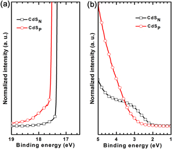
Figure 8. (a) The secondary electron cutoff region and (b) the enlarged highest occupied molecular oribital (HOMO) region of the UPS spectra of the CdS films deposited on the ITO substrates.
Download figure:
Standard image High-resolution image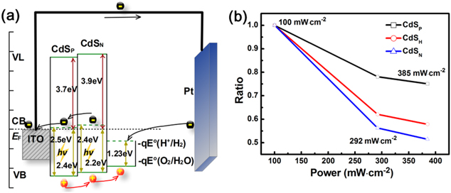
Figure 9. (a) Schematic energy level diagram of the CdSH film in the PEC configuration for water splitting; (b) the ratio of photocurrent efficiency values, with values under 100 mW cm−2 illumination as standard.
Download figure:
Standard image High-resolution image
As an effective photocatalyst, CdSN can easily provide holes to promote the anodic half-reaction under illumination. Correspondingly, the electrons separated from the photogenerated carrier move to the surface of the Pt electrode and drive the cathodic half-reaction, as shown in equation (3).

A fundamental limitation of the alkaline solution is that hydroxyl replaces the hydrogen ion in the cathodic half-reaction. CdSP and CdSH have similar mechanisms in the water splitting process.
Another phenomenon that can exhibit the advantage of CdSH films was also studied. The intense light brings about more photons, which is beneficial for the generation of the photocurrent. It is a very common phenomenon in this type of PEC application. Despite that, the relationship between the light intensity and photocurrent attracts us to pay more attention. Obtained from current densities at a voltage of ∼1 V versus RHE, divided by the power density under various illuminations, the photocurrent efficiency values decrease with the increase of the power densities. All of the detailed parameters can be seen in table S1. Also, the trends of attenuation from a low power density to high power density are obvious in figure 9(b) and in table S2. The normalization of the photocurrent efficiency values makes it clear that the existence of the CdSH film slows the decay of the photoelectric conversion efficiency with the rising power densities.
4. Conclusions
In summary, the integration of two deposition methods to fabricate a CdS NP-neat homojunction film as an efficient photoanode has potential application advantages. The NP grains inside of the CdSH film play an important role in providing more available surface area for catalytic reactions, enhancing the charge separation and suppressing the charge recombination at the interfacial region. The experiment demonstrates the utilization of the CdSH NP film, which results in improvements 22.18 or 3.34 times greater than that of the CdSN or CdSP photoanodes on the photocurrent density in the water splitting process. Further investigation, in accordance with their energy levels, indicates that the suitable band gap of CdS determines its congenital advantages. This systematic study not only serves the methodology innovation that just makes use of the combination of conventional deposition approaches (the ALD and CBD methods) to reach a significant enhancement of the PEC photocurrent density but also gives prominence to the importance of morphology and interfacial energetic control toward enhancing catalytic efficiency. A further investigation on the amount of the H2 and O2 evolution, as well as the time course under certain applied bias-potentials, will be discussed in later works.
Acknowledgments
This work was supported by the 973 program (No. 2014CB932600), NSFC (Nos. 91027041, 612111116, 61107022 and 61007020), the Jiangsu Science and Technology Department (No. BK2011280), the Bureau of Science and Technology of Suzhou Municipality (Nos. SYG201237 and SYG201232), PAPD and the project funded by the China Postdoctoral Science Foundation.