Chipmakers face big challenges at 10nm and beyond

Fifty years after Gordon Moore first described the trend that has driven technology, Intel says scaling is same as it ever was. But other chipmakers, who are struggling to realize the same benefits from good old-fashioned scaling, are increasingly looking for less-expensive alternatives.
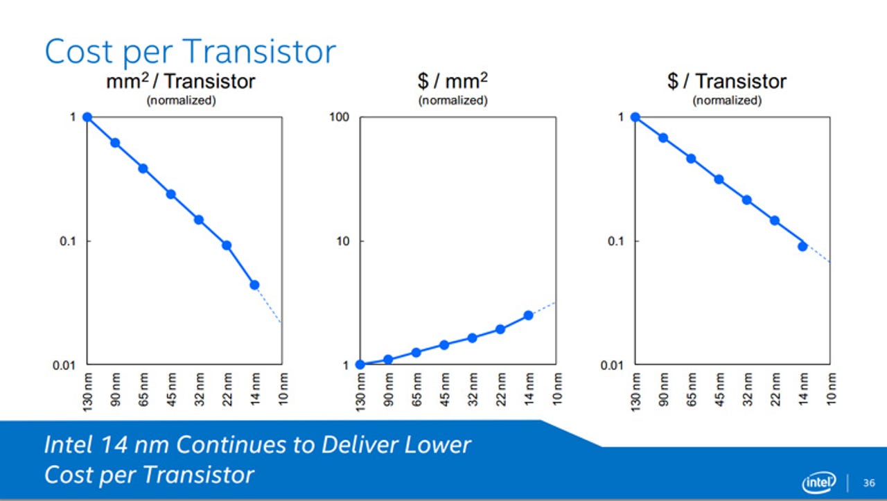
At a panel sessions on the future of Moore's Law at ISSCC, one of the chip industry's main events taking place in San Francisco, Intel's Mark Bohr said that even though "we've all been struggling with increasing rates of wafer costs," the company continued to increase transistor density and reduce cost per transistor at the same rate--perhaps even a little faster at 14nm. He added that the future 10nm and 7nm nodes will also provide both scaling and "ever lower cost per transistor."
This will require new innovation, but Bohr said this has always been the case--most recently with the introduction of high-k materials and metal gates at 45nm and 3D transistors or FinFETs at 22nm. This will take us to 10nm and most likely to 7nm, but beyond that the industry may need more radical solutions including the use of new materials in the channel, the conductive band between the source and drain in a transistor, and new structures such as gate-all-around nanowires or tunnel FETs. The way forward has always seemed "inordinately difficult," Bohr said, but the industry finds a way to continue scaling.
In a separate talk, Kinam Kim, the head of Samsung Semiconductor, said that CMOS transistors should scale down to as low as 3-5nm. But he agreed that it will require some of these new tricks starting around 7nm.
Other companies aren't so convinced that this time isn't different.
Field-programmable gate arrays (FPGAs) have traditionally been one of the key markets for leading-edge technology, but Liam Madden, an executive at Xilinx, pointed out that even if transistors do continue to scale, other parts of the chip such as the metal layers that connect them and the I/O are not scaling. That's why Xilinx is focused on 2.5D and 3D packaging of multiple chips to increase bandwidth and reduce power. While Intel argues advanced packaging is no substitute for scaling, Madden counters that it can reduce cost by replacing one large, complex die with several smaller chips with higher yields that deliver the same performance and features.
TSMC's Jack Sun said the mega-foundry's solution is to do both--chips made with 3D or FinFET transistors stacked in 3D packages (he referred to this as "3D-on-3D"). Separately Xilinx announced its upcoming UltraScale+ devices will use 3D-on-3D including TSMC's 16nm FinFET+ process and 3D chip stacking with through-silicon vias. Designed for wireless, automotive and industrial applications, these new chips will begin shipping in the fourth quarter. The company's rival, Altera, has been developing high-performance Stratix 10 FPGAs and SoCs using Intel's 14nm process with FinFETs.
Qualcomm's Geoffrey Yeap said the industry spends far too much time worrying about scaling, when it should be more focused on adding value that will convince customers to buy a new smartphone or tablet. The company needs to stay around the leading-edge to produce competitive mobile chips, which can be highly complex with not only a CPU, GPU and cellular modems (DSPs), but also RF, connectivity and power management.
But cost is also critical, in particular the time it takes for a new chip design to reach good manufacturing yields. That is why the 28nm node is a "sweet spot" and is likely to be around for a long time (last week Qualcomm announced four new Snapdragon 400 and 600 series processors using TSMC's 28nm process). Yeap said that the 16nm/14nm process with FinFETs also looks like it will be a "good node."
If Qualcomm is having trouble justifying the cost of leading-edge technology, the problem is only magnified for competitors with smaller volumes.
In a separate talk, Sehat Sutardja, the CEO of Marvell, said that because of the escalating costs of R&D and lithography (mask sets), beyond 28nm a chip design would need to reach very high volume (25 million units or more) just to keep costs flat. That might work for Apple, Samsung or Qualcomm but most chipmakers won't see any economic benefits from scaling beyond 28nm.
Marvell's solution to this is a modular design, dubbed MoChi, which combines a Compute chip on the latest process technology with peripheral components, manufactured on older technology for lower cost, connected over an AXI bus with certain extensions. The idea is that the company can assemble these components like Lego bricks to create Virtual SoCs to affordably target different markets such as smartphones, laptops, servers and networking infrastructure.
One of the primary reasons that scaling has become so expensive is that the current lithography tools, which use light with a wavelength of 193nm, can no longer pattern features at these dimensions without multiple passes. The replacement, a next-generation lithography tool that uses extreme ultraviolet (EUV) light with a wavelength of 13.5nm, has been delayed for years and is unlikely to be available for volume production until 7nm (perhaps even later for Intel).
Intel's Bohr said they key question for continued lower cost per transistor was when EUV will be available. The main issues are the source power, which dictates the tool's throughput, and the tool's stability and reliability. This week an industry group is holding its Advanced Lithography conference down the road in San Jose, so expect to hear some news on the progress in these areas.
Barring any major breakthroughs, however, the industry will continue to struggle with higher costs. Intel says it can continue to reduce cost per transistor for the next couple of generations--with or without EUV. But other chipmakers without the same R&D budget and product volumes will increasingly experiment with these sorts of "More than Moore" alternatives to deliver better performance, lower power and more features without breaking the bank.