
Abstract
A three dimensional Monte Carlo simulation program was developed to model physical sputtering and to emulate vias nanomachined by the gas field ion microscope. Experimental and simulation results of focused neon ion beam induced sputtering of copper are presented and compared to previously published experiments. The simulation elucidates the nanostructure evolution during the physical sputtering of high aspect ratio nanoscale features. Quantitative information such as the energy-dependent sputtering yields, dose dependent aspect ratios, and resolution-limiting effects are discussed. Furthermore, the nuclear energy loss and implant concentration beneath the etch front is correlated with the sub-surface damage revealed by transmission electron microscopy at different beam energies.
Export citation and abstract BibTeX RIS
1. Introduction
Innovations in device architecture and nanoscale fabrication technology have enabled device scaling according to Moore's law since 1965. Challenges to instrumentation, methods, analytical tools and many other areas require new synthesis techniques as well as advances in materials and device geometries. The gas field ion source (GFIS) microscope, using helium and neon ions, has garnered much attention recently because of its impact in several critical nanoscale applications such as circuit editing [1, 2], nanoscale imaging [3–7], lithography [8, 9] and nanoscale direct-write synthesis [10–13]. The helium GFIS has demonstrated 0.35 nm image resolution [14], lithography down to 6 nm [15], helium ion beam induced deposition at 10 nm [16] and the milling of sub-10 nm patterns in thin materials such as graphene and gold films [17–20]. Several studies have also been performed to explore the suitability of helium ion beam in backside circuit analysis [21–25]. However, the low atomic weight of helium has some disadvantages for this application. For instance, the low ion mass leads to prohibitively low sputter yields and the low atomic weight of helium leads to a large implant range in the underlying material. Recently the helium and neon sputtering of an alternative nickel extreme ultraviolet (EUV) absorber mask layer was also studied. No discernible helium ion sputtering was observed before severe damage was observed to the underlying EUV reflecting layers; whereas a neon dose of ∼2 × 10¹⁷ ions cm−2 was sufficient to sputter the ∼50 nm nickel layer [26]. The damage profiles for both ion species were correlated to the observed nuclear energy loss and end-of-range implant concentration.
It is generally recognized that many materials cannot be removed effectively by helium sputtering and chemically assisted processes may also be insufficient to etch the myriad of materials of interest. Therefore, much effort has been devoted to make the GFIS technology work with higher mass ion species such as neon. In the past few years, great progress has been made in stabilizing the neon GFIS [27, 28], and recently the neon ion microscope (NIM) had produced a 1–2 nm focused probe size, a few picoamperes of probe current, and stable performance over a period of a few days. Detailed sputter yield characterization of neon shows a sputter rate on the order of 1–4 atoms per incident neon ion at normal incidence, which is about half of what a traditional gallium based FIB provides [6, 23].
To complement and emulate the experimental advances and nanomachining experiments that have been made in the NIM [23, 24], we have expanded our EnvizION simulation [29–31] to investigate physical sputtering. EnvizION is a three dimensional Monte Carlo ion-solid model with nuclear and electronic stopping power algorithms similar to SRIM/TRIM [32, 33]. In this work we have updated the sputtering routines with angle dependent recoil atoms trajectories. In this approach, the scattering direction of a recoil atom depends on the direction cosine of its preceding scattering step instead of considering a random direction for the recoil atoms. The details of the sputtering algorithm are briefly overviewed in simulation methods. In this work we have compared experimental and simulated physical sputtering of copper vias created with 20 keV nanoscale focused neon ion beams. The temporal evolutions of the resultant high-aspect ratio nanostructures are demonstrated and rationalized by tracking the sputtered and re-deposited species. Importantly the nuclear energy loss and implant concentration beneath the etch front of neon ions is correlated with the observed experimental damage revealed by transmission electron microscope (TEM) over a range of neon ion beam energies of 9–34 keV beam. Finally, while the general trends of the simulation correlate well with the experimental results, the observed etching damage front influence on the observed etch rate differences will be discussed, and future simulation directions and algorithm improvements will be elaborated.
2. Experimental methods
The initial experimental copper etch profiles were reported in [24] so only a brief description is provided here. The copper film (∼1 μm) was electron beam evaporated on a 〈100〉 un-doped silicon wafer with a resistivity of 1–10 Ω cm. The focused neon ion beam etch studies were performed on a Zeiss ORION instrument. An FEI Strata 400 Dual Beam was used to prepare TEM samples using a lift-out technique. TEM samples were characterized using a JEOL JEM- 2010 TEM. Before cross-section and TEM sample preparation, 500 nm of platinum were deposited onto the implant region surface by e-beam induced deposition of platinum followed by a 1000 nm platinum deposition by Ga+ ion beam to protect the implant sites from being damaged by the 30 keV Ga+ during the cross-section and TEM sample preparation process.
In order to investigate the copper sputtering process, a 20 keV ∼1 nm full width at half maximum neon ion beam was raster scanned with a 15 pixel scan and 1 nm spacing (15 nm total width) and 500 nm long so cross-section SEM images could be easily made of the resultant etch profile. The pixel dwell time was 1 μs and thus the total loop time was 7.5 ms (dwell time × total number of pixels). Different neon areal doses of 1.5 × 10¹⁸, 3 × 10¹⁸ and 6 × 10¹⁸ Ne+ cm−2 were investigated by simply varying the number of loops. The SEM micrographs of the sputtered profiles were shown previously. To investigate the sub-surface damage and lateral straggle generated during the neon ion etching of copper, another series of copper etches was performed at variable neon ion energy in the range of 9–34 keV with larger line widths of ∼500 nm.
3. Simulation methods
A three dimensional Monte Carlo simulation (EnvizION) [29, 30] was recently updated to investigate the physical sputtering of aluminum and tungsten by using neon and helium ion beams [31]. In this work, we have further updated the method by introducing angle dependent recoil algorithms to better represent the sputtering process. In this approach, the scattering direction of a recoil atom depends on the direction cosine of its preceding scattering step instead of using a random direction for the recoil atoms. The other details of the sputtering algorithm are previously explained [31]. However it is worthwhile to explain the angle dependent approach in this context. Figure 1 is a schematic diagram in which an incident ion (red) scattered from location 1 to location 2. If the ion loses nuclear energy more than the surface binding energy then the target atom at position 2 recoils (blue) and approaches location 3. Two angles θ and ψ as shown in figure 1 are calculated as follows. The angle ψ is calculated as 2πRND where RND is a random number lies between 0 and 1. The angle θ was chosen randomly in the previous work [31] whereas it is calculated as follows in this work.
- (a) Calculate the direction cosines (Cx, Cy, Cz) of the ion while approaching to location 2 from location 1.
- (c) Calculate new direction cosines from the following relations [36]
where
Cp = cos θ, Sp = sin θ, V1 = B.Sp, V2 = B.A.Sp; V3 = cos ψ; V4 = sin ψ, A = (−Cx/Cz) and B = 1/sqrt(1 + A2)
- (d) Calculate the new position of the recoil as xn = x + d. Cx; yn = y + d* Cy; zn = z + d* Cz where d is the step length from positions 2 to 3, and it is calculated as d = −log(RND) × mean free path of the recoil atom [36].

Figure 1. A schematic diagram of the angle-dependent-recoil approach. The red color represents neon ion and the blue shows the recoil atom.
Download figure:
Standard image High-resolution imageAlthough there are many computer simulation programs such as SRIM/TRIM [32, 33], SDTrimSP [34], MC_SIM [37] and Geant4 [38] to model the sputtering process, none of them specifically evolve the topography changes associated with the resultant sputtering; which is extremely important to understanding the nanoscale evolution. Other programs include recoil algorithms and determine the energy-dependent sputtered yield information for the flat surfaces. Additionally, some programs such as AMADEUS [39], IONSHAPER [40] and FIBSIM [41] have been used to calculate/estimate the evolution of the surface. Most of these methods combine ion angular and spatial distribution data from Monte Carlo ion–solid simulations and evolve surface topography in a continuum or cellular manner. The angular and spatial ion distributions, sputtered yields, backscattered ion distribution etc are typically imported from SRIM/TRIM [32, 33] or Geant4 [38]; into the topography simulators such as IONSHAPER [40] or ANETCH [42] etc to study linear trench, prototyping [43] and the structural changes in sputtering [42].
Unlike previous sputtering/profile evolvers, the approach demonstrated here is to directly simulate the topography evolution due to sputtering in the Monte Carlo environment. In this way, a wide range of ions and target combinations as well as scanning parameters and geometries can be directly studied. The only tuning parameter, per se, in the program is the surface binding energy of the target material. As a starting point the heat of sublimation was used for each material, which perhaps fortuitously has yielded very good agreement with the energy-dependent sputter yields. The simulation is capable of tracking sputtered and re-deposited atoms, illustrating the evolution of etched nanostructures. In this research, it is also demonstrated that the evolving energy loss distribution and ion implantation distributions, which are very important to understanding sub-surface damage [21] for various applications can be calculated. It should be noted that this program is ideal for nanoscale focused ion beam induced processing since tractable numbers of ions can reveal important information from the experiments. Larger scale simulations described above become problematic at larger numbers and are more appropriate for microscale applications.
We have investigated the sputtering process of copper by impinging 20 keV neon ions normal to the surface. The surface binding energy of copper was assumed to be of 3.52 eV, which is similar to what SRIM/TRIM uses. A Gaussian shaped beam (at1 nm FWHM) was used for the incident neon ion probe current distribution. The ion beam was simulated to scan over in a 15 nm × 15 nm area at the same doses of 1.5 × 10¹⁸ ions cm−2, 3 × 10¹⁸ ions cm−2 and 6 × 10¹⁸ ions cm−2 as used in the experiment session described above. In the simulation, 1 nm pixel spacing in both the x and y directions, a dwell time of 0.5 μs, and a current of 1 pA were assumed to raster over the patterned region. The atomic voxel size of the copper atoms was assumed to be 0.0121 nm3 based on the atomic mass (63.54 g mol−1) and density (8.96 g cm−3) of copper. For comparison, a simulation at 1.5 × 10¹⁸ ions cm−2 dose was also performed for a 30 nm × 15 nm area to determine the effect of longer lines that were experimentally done (see supplementary document S1).
In order to compare the simulated energy loss profile and implanted ion concentrations to the observed sub-surface damage in copper etched structures, simulations was performed at 9, 12, 20, 25 and 34 keV beam energies. Each simulation included 3 × 10⁵ neon ion trajectories simulated at normal incidence scanned in the same 15 nm × 15 nm area described above (for an equivalent ion dose of 1.33 × 10¹⁷ Ne+ cm−2).
4. Results and discussions
First, the energy dependent sputtered yields of Cu results from EnvizION simulations were compared with SRIM/TRIM. The sputtered yields were calculated as the ratio of the number of sputtered atoms per incident ion. Figure 2 demonstrates the energy dependent sputter yields of copper in a range of 10–35 keV. The EnvizION sputtered yields (black represents the density of 8.96 g cm−3 and blue does the density of 6.5 g cm−3) were calculated by using a 20 nm wide Gaussian beam, using 1.0 × 10⁴ ions on flat substrates at the given energies. The larger FWHM was chosen to avoid deep trench formation, which can affect the resultant sputter yield as described below. The EnvizION sputter yield simulation results are slightly smaller (within ∼10%) than what are estimated by SRIM/TRIM (red color in the figure) over the given energy range. The sputter yields of Cu decrease gradually with increasing beam energies, which is consistent with the fact that the nuclear stopping power decreases with increasing energy, which results in more nuclear energy loss deeper in the target material.
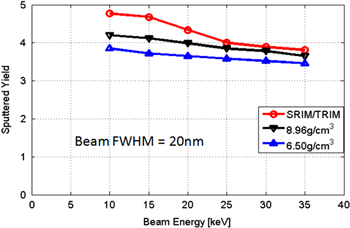
Figure 2. Energy dependent sputtered yields of Cu from SRIM/TRIM (red at density of 8.96 g cm−3) and EnvizION (black for copper density of 8.96 g cm−3). Also included is the simulated (EnvizION) sputter yield for lower density copper (blue at 6.5 g cm−3).
Download figure:
Standard image High-resolution image4.1. Etched nanostructure evolution
In this section, the comparison of the simulation and empirical results on the evolution of the nanostructures in copper at 20 keV beam energy is discussed. Figure 3(a) demonstrates experimental results of the etched nanostructures (cross section SEM micrographs) at three different doses, 1.5 × 10¹⁸ ions cm−2 (a1), 3 × 10¹⁸ ions cm−2 (a2) and 6 × 10¹⁸ ions cm−2 (a3). Figure 3(b) provides the digitized via size and via profile of figure 3(a) at corresponding doses of a1, a2 and a3. The via depths are ∼120 nm (a1), ∼155 nm (a2) and ∼210 nm (a3) whereas the via FWHM are ∼31 nm (a1), ∼30 nm (a2) and ∼30 nm (a3) respectively.

Figure 3. SEM micrographs (left) and via depths versus via widths (right) of sputter etched copper vias. These plots were used with permission for a comparison purpose only. Reproduced with permission from [24]. Copyright 2011, American Vacuum Society.
Download figure:
Standard image High-resolution imageThe simulation results of the copper are shown in figure 4 with the middle slices at three different doses, 1.5 × 10¹⁸ ions cm−2 (a), 3 × 10¹⁸ ions cm−2 (b) and 6 × 10¹⁸ ions cm−2 (c). The simulated via depths at the three doses are ∼152 nm (a), ∼205 nm (b) and ∼272 nm (c), respectively. The corresponding via widths at FWHM are ∼24 nm (a), ∼27 nm (b) and ∼35 nm (c), respectively. We have also added a plot of the summation of the 15 × 15 1 nm FWHM beam profiles to the sputter cross-sections (white dotted Gaussian beam in figure 4).
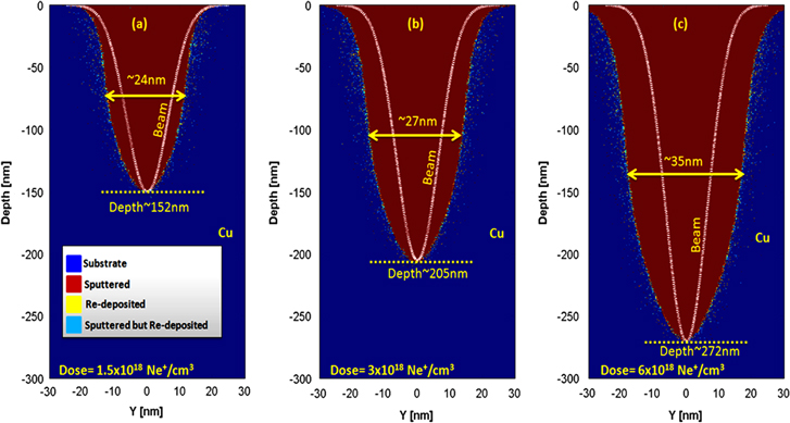
Figure 4. Simulated via structures of Cu at the doses of (a) 1.5 × 10¹⁸ ions cm−2, (b) 3 × 10¹⁸ ions cm−2 and (c) 6 × 10¹⁸ ions cm−2 and the beam energy of 20 keV. The color code: blue (substrate), red (sputtered), yellow (re-deposited) and cyan (sputtered but re-deposited) depict different species. The white dotted curves represent the summation of 15 × 15 Gaussian beams (of 1 nm FWHM) in each plot.
Download figure:
Standard image High-resolution imageThese results from the simulations are in reasonable agreement with the experiments; specifically in both the simulations and experiments the via depths increase ∼30% for each milling dose doubling. An additional simulation for a 15 nm × 30 nm via at the 1.5 × 10¹⁸ ions cm−2 dose was also performed to determine the effect of the extended line scan (did not simulate higher dose due to computational limits). These results and brief description are presented in the supplementary information (S1).
In order to present the better resolutions of the sputtering events the bottom 45 nm of the via structures are plotted in figure 5. Figure 5(a) depicts the middle slice of the bottom part at the doses of 1.5 × 10¹⁸ Ne+ cm−3 and whereas figure 5(b) presents the structure at the dose of 6 × 10¹⁸ Ne+ cm−3.
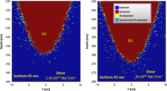
Figure 5. The bottom 45 nm of the middle slice at two different doses. The color code: blue (substrate), red (sputtered), yellow (re-deposited) and cyan (sputtered but re-deposited) depict different species.
Download figure:
Standard image High-resolution imageFigure 6(a) demonstrates the temporal evolutions of sputtered (red), re-deposited (blue) and the sum of the sputtered and re-deposited species (black) of copper during the process. As previously demonstrated [31], the number of sputtered atoms decreases and the re-deposited atoms increases with increasing aspect ratio of the etching via. This observation is correlated to the effective escape angle of the sputtered species. The sputtered versus re-deposited fraction depends on the trajectory of the copper atom. The open-angle varies approximately as 2 × tan−1[(W/2)/d] where W represents the top of the via width and d is the depth. The sputter yield will scale different than the simple open-angle function due to the typical cosine distribution of sputtered species in which the angular distribution of sputtered species is a maximum normal to the substrate. In order to further understand the re-deposited process the via depths are calculated after every one million ions run and the number of re-deposited atoms versus the corresponding depths are presented in figure 6(b). These observation clearly show that the re-deposition events are increasing with increasing depths of the via. Clearly, the rate of re-deposition starts to increase dramatically at 150 nm and begins to saturate at the 250 nm depth where the re-deposited yield approaches the sputter yield with only a small fraction of the atoms being removed.
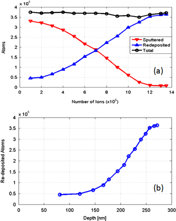
Figure 6. (a) Temporal behavior of sputtered, re-deposited and the sum or total of copper atoms that are displaced as a function of the cumulative number of Ne ions (each data point is sampled every one million ions). (b) Number of re-deposited atoms sampled at every one million ions versus the corresponding via depths.
Download figure:
Standard image High-resolution imageThe difference in the empirical and the simulated sputter yield can be attributed to the damage front that develops and propagates ahead of the etch region. As shown later, the damage front contains implanted Ne, which effectively lowers the density of copper. To illustrate, the energy dependent sputter yield for a lower density copper (6.5 g cm−3) was calculated and also shown in figure 2 (blue). The lower density of the substrate has the effect of reducing the energy loss in the immediate beam entry region which lowers the sputter rates. We plan to add an algorithm to track the evolving density in a manner similar to methods proposed in the TRIDYN simulation [44]. Another mechanism that could be operative is oxidation of copper due to residual water vapor in the vacuum system. Copper oxide has a lower sputter yield thus could retard the sputtering etch rate. In the near future, EnvizION simulation will incorporate the capability of tracking the ion implant concentration and make adaptations to the voxel density and the gas handling algorithms developed for the ion and electron beam induced deposition simulation [30, 45, 46] will be implemented to investigate gas-assisted etching/sputtering.
4.2. Energy loss, surface damage and implant concentrations
Before discussing the specific energy loss and implant concentration for the copper results, it is instructive to demonstrate the penetration depths of a flat copper substrate at various Ne+ energies and compare to EvizION and SRIM/TRIM [35] simulations (excluding sputtering for the EnvizION simulations). The 90% implant range and peak implant depth for both simulations (1.0 × 10⁴ neon ions) are presented in figure 7. The 90% range in figure 7(a) is the distance at which more than 90% of neon ions have stopped. The peak implant depth means the depth at which the implanted neon ion distribution has its maximum concentration. The implant ion distribution is calculated for 9, 12, 20, 25 and 34 keV neon beam energies and the depths of the corresponding maximum peak concentration in the distributions are presented in figure 7(b). These plots demonstrate that the EnvizION results (red) are in excellent agreement with SRIM/TRIM results (black).
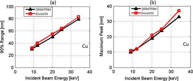
Figure 7. (a) 90% depth range and (b) the maximum implant peaks of Cu at beam energies of 9, 12, 20, 25, and 34 keV for SRIM/TRIM and EnvizION.
Download figure:
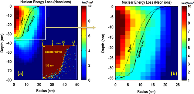
Standard image High-resolution imageIn order to investigate the cumulative nuclear energy loss and implant concentrations, 3.0 × 10⁵ neon ions were simulated using the sputtering algorithm at primary beam energies of 9, 12, 20, 25 and 34 keV on copper substrate in the 15 nm × 15 nm raster scanned area. In these simulations the nuclear, and electronic energy loss, and the implanted ion position, which is the ion location when the ion energy drops below the cutoff energy of 250 eV, are stored for each scattering event. A collage of simulation results for the 20 keV simulation compared to an experimental image of the 20 keV damage profile are illustrated in figure 8. A TEM micrograph figure 8(a) of the bottom of a copper film etched by a neon beam at 1.6 × 10¹⁷ ions cm−2 dose shows a noticeable damage region ∼49 nm beneath the etched nanostructure. The sub-surface radiation damage is characterized by a high concentration of nano bubbles that are associated with copper vacancy coalescence which likely act as a sink for the implanted neon. Figure 8(b) demonstrates the simulated central sputtered etch slice that illustrates an etch depth of ∼13 nm (and a FWHM of ∼16 nm). Figure 8(c) is a plot of the radially averaged nuclear energy loss density as a function of position for the 20 keV simulation, where the color scale represents the logarithm of the nuclear energy loss per volume (eV nm−3). Finally, figure 8(d) illustrates the logarithm of the radially averaged implant concentration as a function of position. The etched material in figures 8(c) and (d) are denoted by the black dotted curves. To correlate the observed damage profile observed in the TEM micrograph (∼49 nm), we note the simulated nuclear energy loss and implant concentration at the experimentally observed damage profile at 49 nm below the bottom of the simulated etched via is ∼1 keV nm−3 and ∼4 × 10²⁰ Ne+ cm−3, respectively. Note that the energy scale less than or equal to 1018 eV nm−3 is given by the same color (dark blue). Similar figures for 9 and 34 keVs are shown in supplemental information (S1) and complementary TEM images for the intermediate energies were also evaluated, but not included for brevity.

Figure 8. (a) TEM micrograph, (b) middle slice of the via, (c) nuclear energy density, (d) implant neon concentration for 20 keV beam energy on copper. The dotted black curves represents the sputtered area of copper in figures (c) and (d) respectively. The affected area in TEM micrograph (a) is also highlighted.
Download figure:
Standard image High-resolution imageFigure 9(a) is a plot of the experimentally observed sputter depths (extrapolated from 1.3 × 10¹⁸ Ne+ cm−2 doses) and the measured sub-surface damage depth versus Ne+ energy. The sputtered depth trends are similar for the simulated and experimental results and as expected, both decrease with increasing energy over the energy range studied. To compare the sub-surface damage depth, figure 9(b) includes the depth below the bottom of simulated the sputter via in which the nuclear energy density is approximately 1 keV nm−3 and the depth at which the implant concentration is 4 × 10²⁰ Ne+ cm−3. Clearly the observed experimental damage profile correlates well with both of these simulation outputs. The spatial trends in the simulated nuclear energy loss and implant concentrations also agree with the experimental damage profiles. Namely, the radiation damage and apparent nano bubble size is greatest near the surface which agrees well with the implant concentration profile. Importantly, whereas a static non-evolving implant simulations predict a maximum implant concentration deeper into the substrate (for instance figure 7(b)), the evolving implant concentration illustrates that a peak in the ion concentration (and nuclear energy loss) is just beneath the surface [26].

Figure 9. (a) Experimental and simulated sputter depths, and damage depths at 9, 12, 20, 25 and 34 keV on copper for 1.3 × 10¹⁷ Ne+ cm−2, (b) simulated nuclear energy density and implant neon concentrations for the given energy. The left y-axis represents nuclear energy loss density and the right y-axis depicts the implant neon ion concentrations in figure 9(b).
Download figure:
Standard image High-resolution imageClearly, both the nuclear energy loss density and implant concentration play important roles in the sub-surface damage. The bombardment of energetic particles and ion implantation produced lattice disorder cause well-known irradiation-induced defects. These defects can be point defect clusters, dislocation loops, stacking fault tetrahedra, interstitials, vacancies and voids depending on the irradiation conditions such as temperature, dose, dose rate and ion species and incident energies [47–50]. In addition to these defects a by-product of neon irradiation induced lattice damage, which is insoluble in most metals and whose atoms can combine with the vacancies to form pressurize bubbles [49]. Studies of neon implantation into copper show the production of dislocations, dislocation loops and mono-vacancies, which can be annealed out during a heat treatment at temperatures up to 623 K. Concurrently, the implanted neon atoms migrate into the large size voids created by the implantation damage and transform into bubbles [47]. These and other irradiation-induced defects cause degradation in the mechanical properties of metals such as embrittlement and void swelling [49]. Novel material systems are required to promote the annihilation and recombination of point defects, suppress bubble formation and prevent blistering and void formation [50]. Recently Rudneva et al showed that nanoscale helium etching of strontium titanate and silicon at elevated temperatures was sufficient to eliminate notable swelling when similarly done at room temperature [51]. These and other strategies will perhaps need to be developed to mitigate some of the damage induced in the beam range when editing devices or preparing specimens.
Consistent with what we observe in the Ne-copper system, recently we showed that the observed damage in 40 pairs of Mo–Si bi-layers (∼2.5 and 3.5 nm thick, respectively) used for EUV reflective masks when exposed He+ and Ne+ could be correlated to both the nuclear energy loss and the implant concentration [26]. In this bi-layer material system, two correlations were made, namely: (1) intermixing of the Mo–Si layers was correlated to nuclear energy loss suspected to be caused by knock-on collisions; and (2) at higher doses, the implanted ion concentration was correlated to nanoscale bubble formation from presumably coalesced inert ions.
Based on results from the EnvizION Monte Carlo simulation, we can comment both on sputtering rate-limiting and resolution-limiting effects in the focused Ne+ beam induced sputtering of copper. The rate-limiting effects are attributed to: (1) the damage front that emerges and effectively decreases the density of the copper material thus decreasing the sputter yield; and (2) re-deposition of copper at high aspect ratios which lowers the amount of material that is sputtered from the via. The resolution-limiting effects can be illustrated by comparing a simulation of the sputter profile and the resultant energy loss density as shown in figure 10. Figure 10 compares the sputter profile and the energy loss for a 702 k neon ions simulation (3.12 × 10¹⁷ Ne+ cm−2) assuming a 1 nm pixel spacing and the 15 × 15 1 nm FWHM (only run to 702 k ions because the energy loss algorithm is computationally demanding). Also included for comparison is the summation of the 15 × 15 Gaussian beams to demonstrate the ideal resolution (dotted line indicated as beam in figure 10(a)). For clarity, the etched profile is overlaid in figure 10(a) on the energy loss density plot. Basically the resolution is limited first of all by the lateral straggle and energy loss of the ion beam. Thus the energy loss distribution is critical to the resolution of the resultant profile and both the vertical and lateral threshold for sputtering appears to be ∼5.5 keV nm−3 as shown in figure 10(b). The dark blue color in figure 10(b) represents the energy loss density which is less or equal to 1 keV nm−3. Secondly, as the rate decreases due to re-deposition, the beam tails of the Gaussian are effectively amplified (or the peaks decreased), which can further compromise the resolution at high-aspect ratios.
Figure 10. Nuclear energy loss density at Cu target with 702 000 neon ions (a dose of 3.12 × 10¹⁷ Ne+ cm−2) of 20 keV. The inner plot of (a) depicts the sputtering profile and figure 10(b) is a zoomed region of the rectangle shown in (a). The dark blue color of figure 10(b) represents nuclear energy loss of 1 keV nm3 or less.
Download figure:
Standard image High-resolution image
5. Conclusions
A three dimensional Monte Carlo method for simulating physical sputtering was developed in order to study vias nanomachined by the neon GFIS. Simulation results of nanoscale sputtered vias in copper were compared to experimental results. The simulated via depths and FWHM were in a good agreement with experiments. The deviation in the absolute sputtering depths is attributed to the lower density in the damage front region as well as possible oxidation during the experimental sputtering. The observed energy-dependent damage front was correlated to the the nuclear energy loss density of ∼1 keV nm−3 on copper substrate at a critical implant concentration of 4 × 10²⁰ Ne+ cm−3.
Acknowledgments
RT and PDR would like to acknowledge support of the Semiconductor Research Corporation (Bob Havemann program manager) and Intel Corporation. PDR also acknowledges that some of the original Monte Carlo algorithms were developed at the Center for Nanophase Materials Sciences, which is sponsored at Oak Ridge National Laboratory by the Scientific User Facilities Division, Office of Basic Energy Sciences, US Department of Energy.